Preparation method of field stop insulated-gate bipolar transistor

A technology of bipolar transistors and insulated gates, applied in the manufacture of semiconductor/solid-state devices, electrical components, circuits, etc., can solve the problems that the field stop layer cannot be obtained, the activation rate is greatly affected by temperature changes, and the overall performance of the device is affected.

Active Publication Date: 2016-07-20
CSMC TECH FAB2 CO LTD
View PDF4 Cites 2 Cited by
  • Summary
  • Abstract
  • Description
  • Claims
  • Application Information

AI Technical Summary

Problems solved by technology

[0002] The traditional fabrication method of field-stop insulated gate bipolar transistor (FS-IGBT) devices usually adopts the front-side process first, and then introduces the field-stop (FS) layer by back injection after the back sheet. Since the front metal pattern must be protected, annealing The temperature should not be too high (generally no more than 450°C). Under such low-temperature annealing conditions, the impurities implanted into the FS layer can not only push the junction but also have a very low activation rate, and the activation rate is greatly affected by temperature changes, and the required concentration cannot be obtained. distributed field stop layer
These issues can seriously affect the overall performance of the device

Method used


Image

  • Preparation method of field stop insulated-gate bipolar transistor
  • Preparation method of field stop insulated-gate bipolar transistor
  • Preparation method of field stop insulated-gate bipolar transistor

Examples


Embodiment Construction

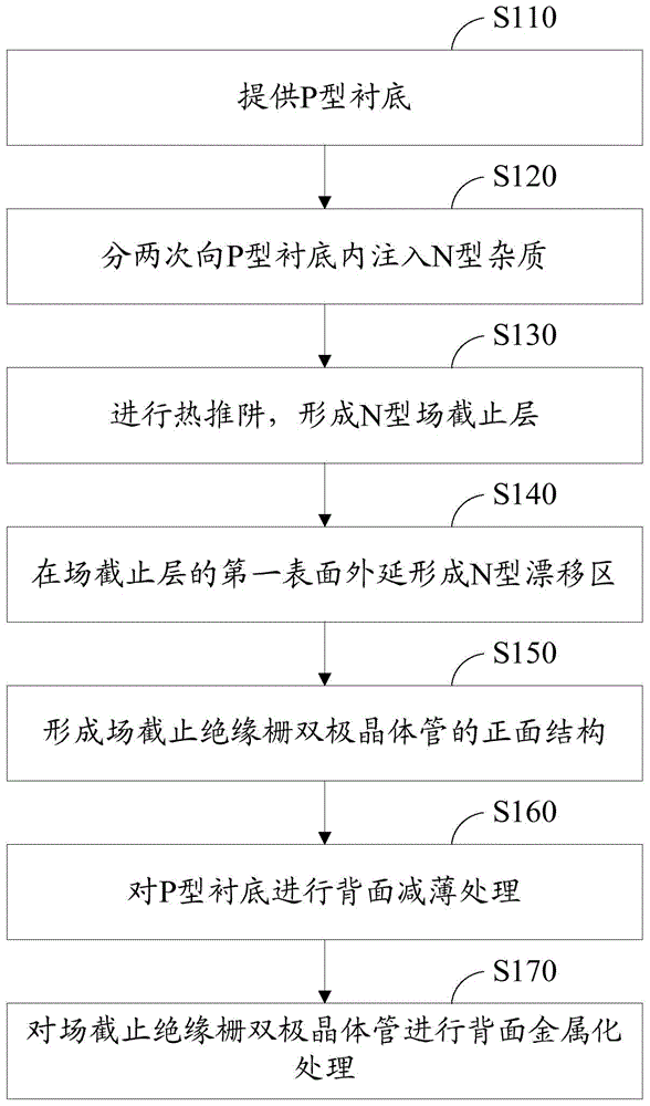
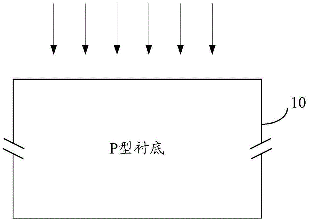
[0018] In order to facilitate the understanding of the present invention, the present invention will be described more fully below with reference to the relevant drawings. The preferred embodiment of the invention is shown in the drawings. However, the present invention can be implemented in many different forms and is not limited to the embodiments described herein. On the contrary, the purpose of providing these embodiments is to make the disclosure of the present invention more thorough and comprehensive.

[0019] It should be noted that when an element is referred to as being "fixed to" another element, it can be directly on the other element or a central element may also exist. When an element is considered to be "connected" to another element, it can be directly connected to the other element or an intermediate element may be present at the same time. The terms "vertical", "horizontal", "upper", "lower", "left", "right" and similar expressions used herein are for illustra...


PUM


Abstract

The invention provides a preparation method of a field stop insulated-gate bipolar transistor. The method comprises the steps as follows: a P-type substrate is provided; N-type impurities are implanted into the P-type substrate twice, namely one-time arsenic ion implantation and one-time phosphorus ion implantation; the implantation energy of phosphorus ion implantation is greater than that of arsenic ion implantation; heat diffusion is carried out to form an N-type field stop layer; an N-type drift region is formed on the first surface of the field stop layer in an epitaxy manner; a front-side structure of the field stop insulated-gate bipolar transistor is formed; back thinning treatment is carried out on the P-type substrate; and back metalized treatment is carried out on the field stop insulated-gate bipolar transistor. By one-time low-energy arsenic implantation and one-time high-energy phosphorus implantation, N-type impurity concentration distribution of a field stop layer can be optimized by the difference between the arsenic ion diffusion rate and the phosphorus ion diffusion rate during twice implantation.

Description

Technical field [0001] The invention relates to the technical field of semiconductor preparation, in particular to a method for preparing a field stop insulated gate bipolar transistor. Background technique [0002] The traditional field stop insulated gate bipolar transistor (FS-IGBT) device preparation method usually adopts the front side process first, and then the back side sheet and back injection method to introduce the field stop (FS) layer. To protect the front metal pattern, annealing The temperature cannot be too high (generally not more than 450°C). Under such low temperature annealing conditions, the impurity injected into the FS layer not only cannot push the junction, but the activation rate is very low, and the activation rate is greatly affected by temperature changes, and the required concentration cannot be obtained. Distributed field stop layer. These problems will seriously affect the overall performance of the device. Summary of the invention [0003] Based ...

Claims


Application Information

Patent Timeline
Patent Type & Authority Applications(China)
IPC IPC(8): H01L21/331H01L21/265
Inventor 钟圣荣王根毅邓小社周东飞
Owner CSMC TECH FAB2 CO LTD
Why Eureka
Try Eureka