Semiconductor storage device including a gate insulating film with a favorable nitrogen concentration profile and method for manufacturing the same

a technology of nitrogen concentration profile and semiconductor storage device, which is applied in the direction of semiconductor devices, basic electric elements, electrical equipment, etc., can solve the problems of difficult to form an appropriate nitrogen concentration profile, difficult to control the formation of nitrogen peaks, and deterioration of transistor characteristics, etc., to achieve favorable nitrogen concentration profile, excellent electrical characteristics, and excellent electrical characteristics

Inactive Publication Date: 2011-11-29
TOKYO ELECTRON LTD +1
View PDF17 Cites 2 Cited by
  • Summary
  • Abstract
  • Description
  • Claims
  • Application Information

AI Technical Summary

Benefits of technology

[0006]Accordingly, an object of the present invention is to provide a method for fabricating a semiconductor storage de vice with excellent electrical characteristics (write / erase characteristics) by means of a favorable nitrogen concentration profile of a gate insulating film.
[0054]According to the present invention, nitrogen peaks can be formed simultaneously on the surface and interface sides of the gate insulating film of the semiconductor storage device (flash memory) (see FIG. 4). In this case, the use of an oxynitriding species (a gas for oxynitriding species) previously diluted by plasma excitation as is preferred. If the concentration of the nitrogen peaks formed at each interface of the gate insulating film is 0.5 atomic % or less, excellent electrical characteristics can be obtained. Furthermore, it was confirmed that by performing plasma processing in the absence of hydrogen, electron capture characteristics are improved, and the write / erase characteristics of flash memory are also improved.

Problems solved by technology

However, this causes deterioration in transistor characteristics, and causes a nitrogen peak to form only at the interface between the oxide film and the substrate, thus it is difficult to form an appropriate nitrogen concentration profile.
In other words, when thermal oxynitridation is performed nitrogen peaks are formed at specific locations with a specific concentration, and the formation of these nitrogen peaks is difficult to control.

Method used


Image

  • Semiconductor storage device including a gate insulating film with a favorable nitrogen concentration profile and method for manufacturing the same
  • Semiconductor storage device including a gate insulating film with a favorable nitrogen concentration profile and method for manufacturing the same
  • Semiconductor storage device including a gate insulating film with a favorable nitrogen concentration profile and method for manufacturing the same

Examples


Embodiment Construction

[0021]The present invention is applicable to a semiconductor storage device (flash memory, EEPROM or the like) which operates by transferring a charge through an insulating film.

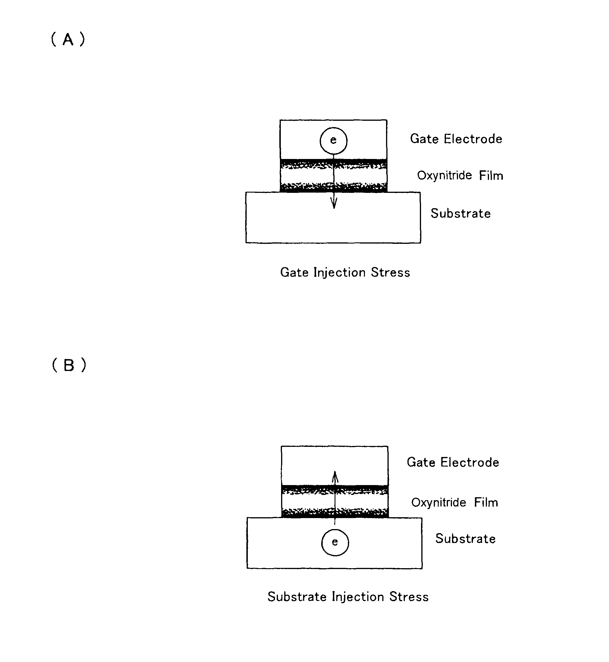
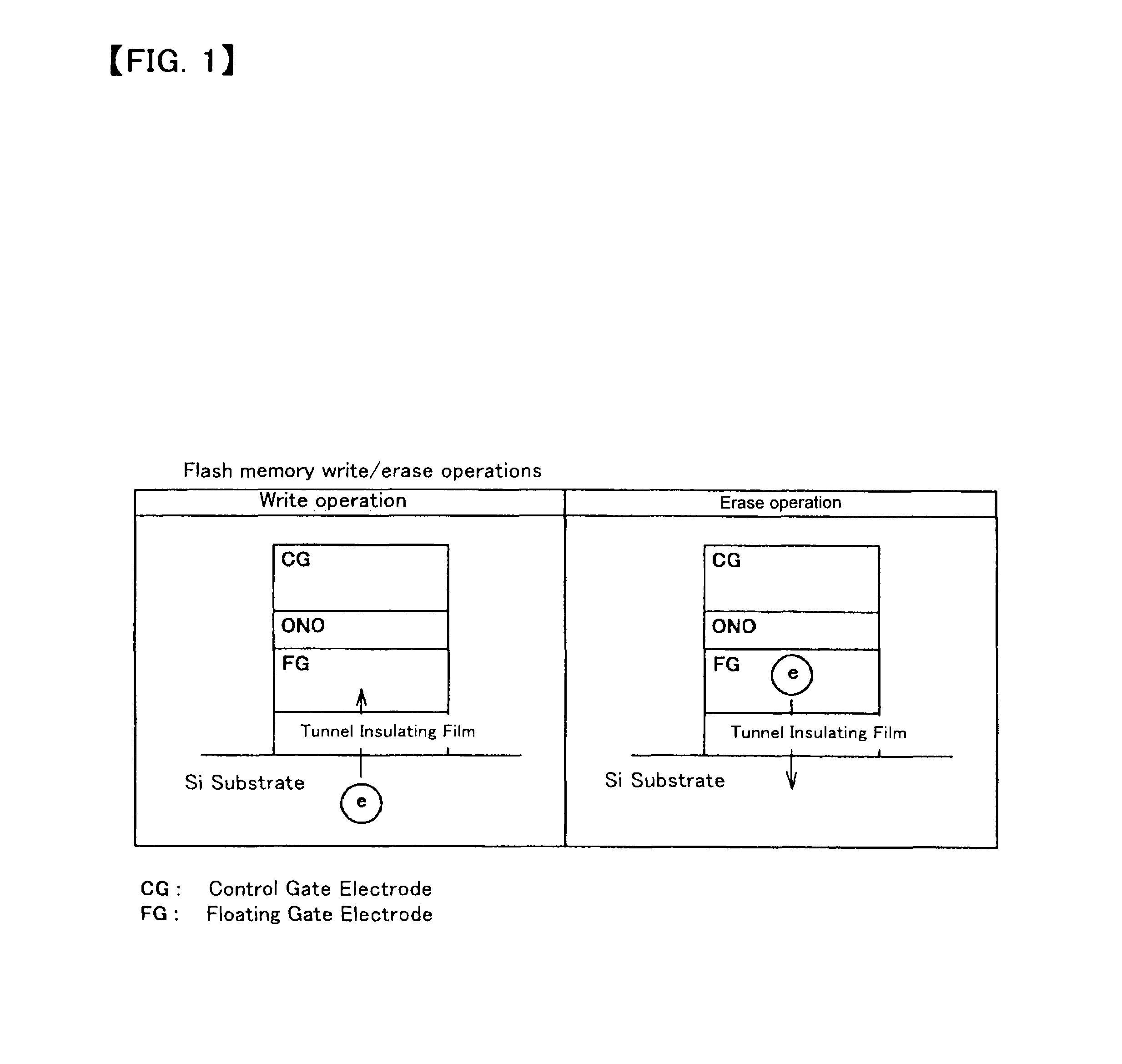
[0022]FIG. 1 is an explanatory diagram showing examples of write and erase operations in flash memory, representing an application of the present invention. During a write operation, a charge flows from a silicon substrate to a gate electrode (FG: Floating Gate) through a tunnel insulating film. On the other hand, during an erase operation, a charge flows from the gate electrode (FG) to the silicon substrate through the tunnel insulating film. The present invention is characterized by the structure (nitrogen concentration profile) of the tunnel insulating film (gate insulating film).

[0023]To avoid damaging the gate insulating film, plasma processing of the film is performed using an RLSA (Radial Line Slot Antenna) microwave plasma processing apparatus, which produces a high density plasma with a low electron...


PUM


Abstract

A semiconductor storage device with excellent electrical characteristics (write / erase characteristics) by favorable nitrogen concentration profile of a gate insulating film, and a method for manufacturing the semiconductor device. The semiconductor device fabricating method operates by transferring charges through a gate insulating film formed between a semiconductor substrate and a gate electrode, including introducing an oxynitriding species previously diluted by plasma excitation gas into a plasma processing apparatus, generating an oxynitriding species by a plasma, and forming an oxynitride film on the semiconductor substrate as the gate insulating film. The oxynitriding species contains NO gas at a ratio of 0.00001 to 0.01% to the total volume of gas introduced into the plasma processing apparatus.

Description

TECHNICAL FIELD[0001]The present invent on relates to a semiconductor storage element (flash memory, EEPROM or the like) which operates by transferring a charge through an insulating film, and relates particularly to an improved method of forming a gate insulating film for placement between a semiconductor substrate and a gate electrode.BACKGROUND ART[0002]In relation to the electrical characteristics (write / erase characteristics) of a semiconductor storage device, the nitrogen concentration profile of the gate insulating film is of great significance. Conventionally, a thermal oxynitridation process is carried out to oxide films. However, this causes deterioration in transistor characteristics, and causes a nitrogen peak to form only at the interface between the oxide film and the substrate, thus it is difficult to form an appropriate nitrogen concentration profile. In other words, when thermal oxynitridation is performed nitrogen peaks are formed at specific locations with a speci...

Claims


Application Information

Patent Timeline
Patent Type & Authority Patents(United States)
IPC IPC(8): H01L21/02
CPCH01L21/28202H01L21/28273H01L29/513H01L29/792H01L29/40114H10B99/00
Inventor KITAGAWA, JUNICHIOZAKI, SHIGENORITERAMOTO, AKINOBUOHMI
Owner TOKYO ELECTRON LTD
Why Eureka
Try Eureka