Thermal protect pcram structure and methods for making

A technology of memory and memory components, applied in static memory, digital memory information, information storage, etc., can solve the problems of resistive switching performance attenuation, composition change, memory cell failure, etc.

Active Publication Date: 2011-01-26
MACRONIX INT CO LTD
View PDF16 Cites 0 Cited by
  • Summary
  • Abstract
  • Description
  • Claims
  • Application Information

AI Technical Summary

Problems solved by technology

[0009] In addition, higher current levels can cause problems like localized heating, which is sufficient to cause diffusion / reaction of electrodes and phase change materials, and / or cause compositional changes of phase change materials in the active region, which leads to degradation of resistive switching performance and the failure of the storage unit may

Method used


Image

  • Thermal protect pcram structure and methods for making
  • Thermal protect pcram structure and methods for making
  • Thermal protect pcram structure and methods for making

Examples


Embodiment Construction

[0029] refer to Figures 1 to 11 Embodiments of the present invention will be described in detail.

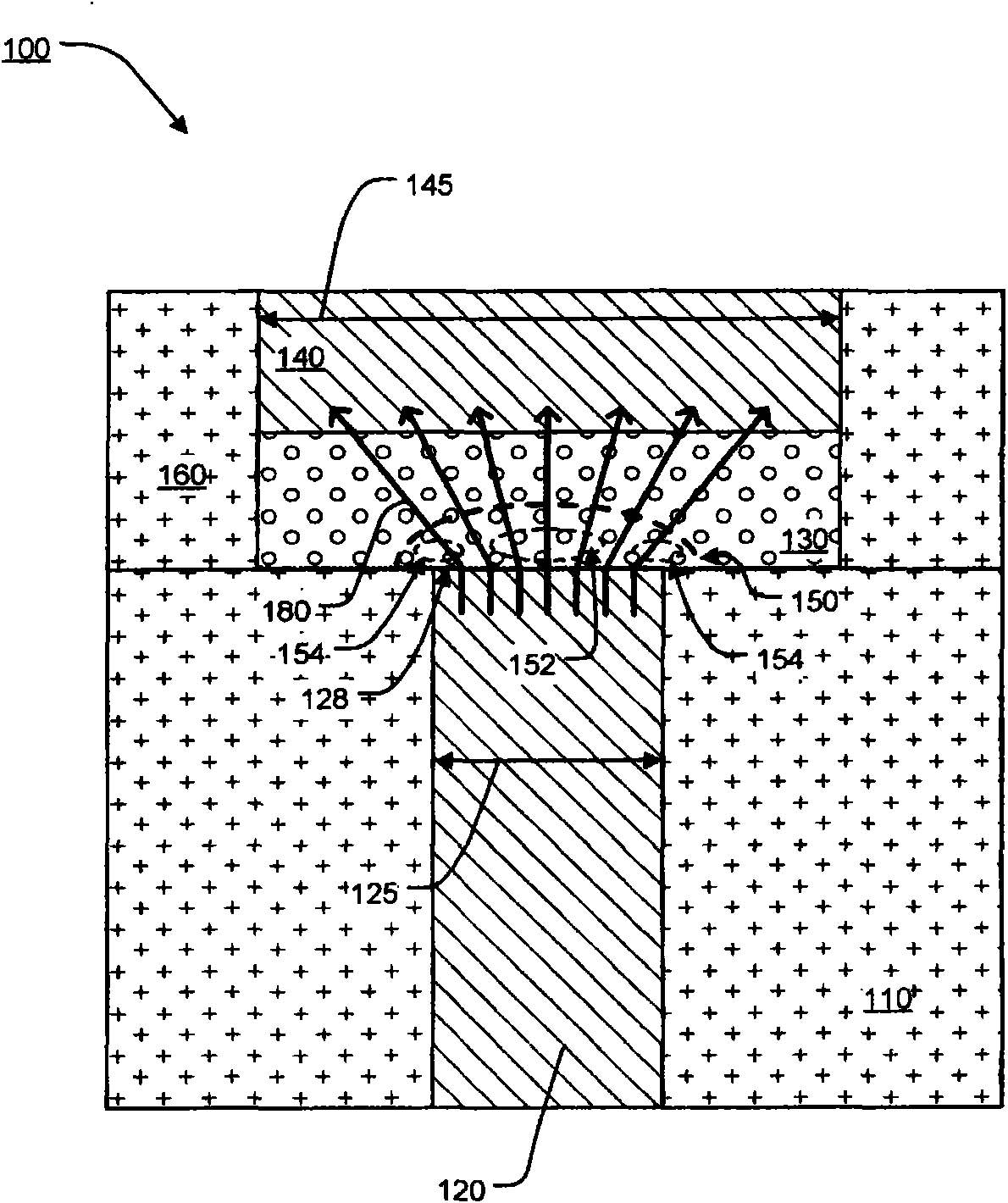
[0030] figure 1 Shown is a cross-sectional view of a known art "mushroom-type" memory cell 100 having a bottom electrode 120 extending through a dielectric layer 110; a phase-change memory element 130 including a bottom electrode 120 a phase change material layer on the top; and the top electrode 140 on the phase change memory element 130 . A dielectric layer 160 surrounds the phase change memory element 130 . as available from figure 1 It can be seen that the width 125 of the bottom electrode 120 is smaller than the width 145 of the top electrode 140 and the phase change memory element 130 .

[0031] In operation, the voltage on the top and bottom electrodes 140, 120 induces a current to flow from the top electrode 140, through the phase change memory element 130, to the bottom electrode 120, or in the opposite direction.

[0032] Active region 150 refers to the region of...


PUM


Abstract

A memory cell as described herein includes a conductive contact and a memory element comprising programmable resistance memory material overlying the conductive contact. An insulator element extends from the conductive contact into the memory element, the insulator element having proximal and distal ends and an inside surface defining an interior. The proximal end is adjacent the conductive contact. A bottom electrode contacts the conductive contact and extends upwardly within the interior from the proximal end. The memory element is within the interior extending downwardly from the distal end to contact a top surface of the bottom electrode at a first contact surface. A top electrode can be separated from the distal end of the insulator element by the memory element and contact the memory element at a second contact surface having a surface area greater than that of the first contact surface.

Description

technical field [0001] The present invention relates to a memory device based on a phase-change memory material and a manufacturing method thereof. The phase-change memory material includes a chalcogen compound material, or other programmable resistance material. Background technique [0002] Phase change memory materials, such as chalcogenide-based materials and the like, can be changed between amorphous and crystalline states by applying a current at a level suitable for integrated circuit implementation. The generally amorphous state is characterized by a higher resistivity than the generally crystalline state, which can be easily sensed to indicate data. These properties are of interest in the use of programmable resistive materials to form non-volatile memory circuits that can be read and written randomly. [0003] The change from amorphous to crystalline state is generally a lower current operation in which the current heats the phase change material above the transit...

Claims


Application Information

Patent Timeline
Patent Type & Authority Applications(China)
IPC IPC(8): H01L45/00H01L27/24G11C11/56
CPCH01L27/2436H01L45/04H01L45/147H01L45/1246H01L45/146H01L45/085H01L45/06H01L45/144H01L45/148H01L45/1683H01L45/142H01L45/1625H01L45/1233H10B63/30H10N70/245H10N70/828H10N70/231H10N70/20H10N70/8822H10N70/826H10N70/8836H10N70/884H10N70/8828H10N70/8833H10N70/026H10N70/066
Inventor 陈士弘
Owner MACRONIX INT CO LTD
Why Eureka
Try Eureka