Novel adiabatic logic gating circuit

A logic gate circuit and adiabatic technology, applied in the field of logic gate circuit, can solve problems such as energy consumption, achieve ultra-low power consumption, and reduce circuit power consumption

Inactive Publication Date: 2012-07-25
NINGBO UNIV
View PDF0 Cites 1 Cited by
  • Summary
  • Abstract
  • Description
  • Claims
  • Application Information

AI Technical Summary

Problems solved by technology

In a traditional static CMOS circuit, when the input signal jumps, the DC power supply charges the capacitance of a certain node to Vdd, which means that the stored signal energy is The energy delivered by the power supply to the circuit node is Obviously, in addition to half of the energy delivered to the nodes, half of the energy is dissipated

Method used


Image

  • Novel adiabatic logic gating circuit
  • Novel adiabatic logic gating circuit
  • Novel adiabatic logic gating circuit

Examples


Embodiment 1

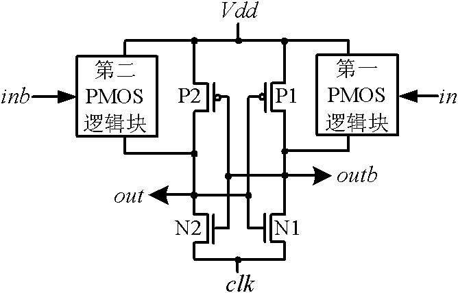
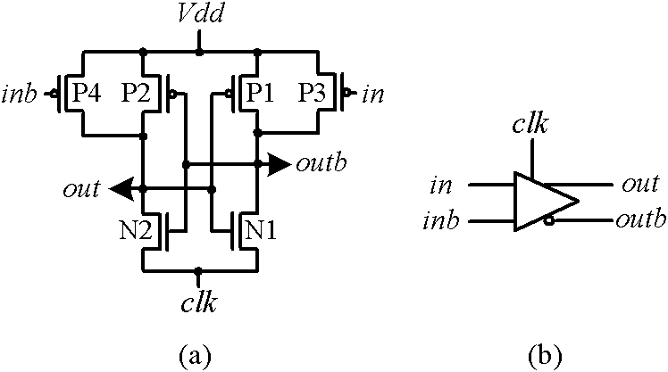
[0030] Embodiment 1: A novel adiabatic logic basic gate buffer (or inverter) circuit, comprising a first PMOS transistor P1, a second PMOS transistor P2, a first NMOS transistor N1 and a second NMOS transistor N2, the first PMOS transistor The source of P1 and the drain of the second PMOS transistor P2 are connected to the positive power supply terminal Vdd in parallel, the source of the first NMOS transistor N1 and the drain of the second NMOS transistor N2 are connected in parallel to the clock signal terminal clk, and the first PMOS transistor The drain of P1 is connected to the drain of the first NMOS transistor N1 and connected to the negative output signal terminal outb, the source of the second PMOS transistor P2 is connected to the source of the second NMOS transistor N2 and connected to the positive output signal terminal out, The gate of the first PMOS transistor P1 and the gate of the first NMOS transistor N1 are connected in parallel to the positive output signal te...

Embodiment 2

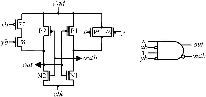
[0031] Embodiment 2: A novel adiabatic logic AND gate circuit, comprising a first PMOS transistor P1, a second PMOS transistor P2, a first NMOS transistor N1 and a second NMOS transistor N2, the source of the first PMOS transistor P1 and the second PMOS transistor The drain of the transistor P2 is connected to the positive power supply terminal Vdd in parallel, the source of the first NMOS transistor N1 and the drain of the second NMOS transistor N2 are connected to the clock signal terminal clk in parallel, and the drain of the first PMOS transistor P1 is connected to the first NMOS The drain of the transistor N1 is connected to the negative output signal terminal outb at the same time, the source of the second PMOS transistor P2 is connected to the source of the second NMOS transistor N2 and connected to the positive output signal terminal out, and the gate of the first PMOS transistor P1 The gate of the first NMOS transistor N1 is connected to the positive output signal term...

Embodiment 3

[0032] Embodiment 3: A novel adiabatic logic OR gate circuit, comprising a first PMOS transistor P1, a second PMOS transistor P2, a first NMOS transistor N1 and a second NMOS transistor N2, the source of the first PMOS transistor P1 and the second PMOS transistor The drain of the transistor P2 is connected to the positive power supply terminal Vdd in parallel, the source of the first NMOS transistor N1 and the drain of the second NMOS transistor N2 are connected to the clock signal terminal clk in parallel, and the drain of the first PMOS transistor P1 is connected to the first NMOS The drain of the transistor N1 is connected to the negative output signal terminal outb at the same time, the source of the second PMOS transistor P2 is connected to the source of the second NMOS transistor N2 and connected to the positive output signal terminal out, and the gate of the first PMOS transistor P1 The gate of the first NMOS transistor N1 is connected to the positive output signal termi...


PUM


Abstract

The invention discloses a novel adiabatic logic gating circuit. A first p-channel metal oxide semiconductor (PMOS) tube, a second PMOS tube, a first n-channel metal oxide semiconductor (NMOS) tube, and a second NMOS tube form an energy recovery circuit with a cross-coupled structure, the source electrode of the first PMOS tube and the drain electrode of the second PMOS tube are parallelly connected to the positive terminal of a power source, the source electrode of the first NMOS tube and the drain electrode of the second NMOS tube are parallelly connected to a clock signal terminal, a first PMOS logic block is bridged between the source electrode of the first PMOS tube and the drain electrode of the first PMOS tube, a second PMOS logic block is bridged between the drain electrode of the second PMOS tube and the source electrode of the second PMOS tube, the first PMOS logic block is provided with at least one positive input signal connecting terminal, and the second PMOS logic block is provided with at least one inverted input signal connecting terminal. The invention has the advantages that: an adiabatic circuit of which the functional characteristics are completely opposite to those of the traditional adiabatic logic circuit is provided, and the first PMOS logic block and the second PMOS logic block consists of PMOS tubes, so that the circuit power consumption can be greatlyreduced.

Description

technical field [0001] The invention relates to a logic gate circuit with low power consumption performance, in particular to a novel adiabatic logic gate circuit. Background technique [0002] With the rapid development of integrated circuit manufacturing technology, especially in the ultra-deep submicron era, power consumption has become a non-negligible limiting factor in VLSI system design. In a traditional static CMOS circuit, when the input signal jumps, the DC power supply charges the capacitance of a certain node to Vdd, which means that the stored signal energy is The energy delivered by the power supply to the circuit node is Obviously, in addition to half of the energy delivered to the nodes, half of the energy is consumed. When the node is pulled low, the charge is released from the node to the ground, that is, half of the energy injected into the node is also consumed. It can be seen that the energy drawn from the power supply is only utilized once. Theref...

Claims


Application Information

Patent Timeline
Patent Type & Authority Patents(China)
IPC IPC(8): H03K19/00
Inventor 胡建平刘彬彬陈金丹邬杨波
Owner NINGBO UNIV
Why Eureka
Try Eureka