Semiconductor memory device

A storage device and semiconductor technology, applied in information storage, static memory, digital memory information, etc., can solve problems such as long pre-charging time, and achieve the effect of preventing malfunction, realizing action, and stabilizing action

Active Publication Date: 2013-01-30
SOCIONEXT INC
View PDF1 Cites 0 Cited by
  • Summary
  • Abstract
  • Description
  • Claims
  • Application Information

AI Technical Summary

Problems solved by technology

However, when the power supply voltage is Vdd and the threshold voltage of the NMOS transistor is Vtn, a long precharge time is required to raise the potential of the signal line to Vdd-Vtn through the NMOS transistor.

Method used


Image

  • Semiconductor memory device
  • Semiconductor memory device
  • Semiconductor memory device

Examples


Embodiment Construction

[0054] Hereinafter, embodiments of the present invention will be described in detail with reference to the drawings. Here, the same symbols are assigned to the same parts in the configuration of the IO module, and repeated explanations are omitted.

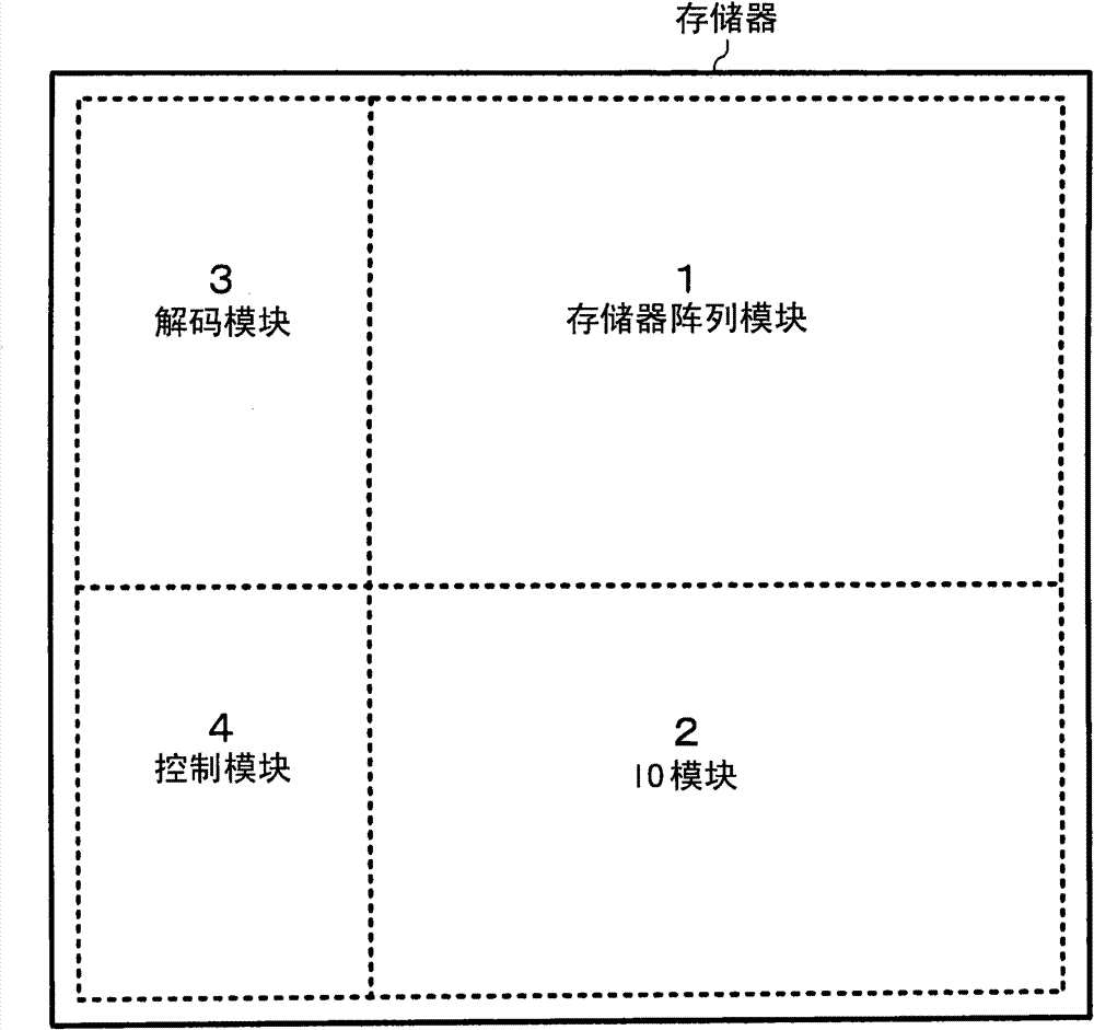
[0055] figure 1 A configuration example of an SRAM module which is one of the semiconductor memory devices according to the present invention is shown. figure 1 The memory array module 1 is a configuration in which a plurality of memory cells are arranged in a matrix, and is equipped with an IO module 2 arranged for a column of the memory array module 1, and a decoding module 3 arranged for a row of the memory array module 1, and is connected with The adjacent positions of the IO module 2 and the decoding module 3 are further configured with a control module 4 .

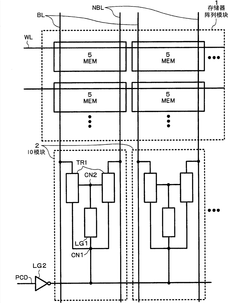
[0056] figure 2 expressed figure 1 The detailed structure of memory array module 1 and IO module 2. exist figure 2 Among them, the memory array module 1 has: a p...


PUM


Abstract

A memory to which a bit line potential step-down technique is applied is provided. The memory includes an IO block including first transistors which control potentials of first bit lines provided with respect to columns of memory cells, and first logic gates which control the first transistors. The drain or source of each first transistor is connected to an input of the corresponding first logic gate, and the gate of each first transistor is connected to an output of the corresponding first logic gate. The first transistors are driven by pulses.

Description

technical field [0001] The present invention relates to a semiconductor memory device, in particular to a technology for controlling the potential of a bit line of a memory circuit. Background technique [0002] Conventionally, in order to improve the SNM (Static Noise Margin) of the memory cell of the SRAM (Static Random Access Memory), there is known a method in which an N-channel MOS (NMOS) transistor connected to a bit line is pulse-driven to lower the voltage of the bit line. technology. Among them, as a data reading method, a sense amplifier that detects a slight potential difference between a pair of bit lines is used (see Non-Patent Document 1). [0003] On the other hand, there is also known a technique for controlling the potential level of a signal line by using a decoding circuit unit for driving a word line of a semiconductor memory device (see Patent Document 1). [0004] Patent Document 1: Japanese Patent Laid-Open No. 2007-164922 [0005] Non-Patent Docume...

Claims


Application Information

Patent Timeline
Patent Type & Authority Patents(China)
IPC IPC(8): G11C11/41G11C11/413G11C11/417
CPCG11C11/419G11C7/12
Inventor 增尾昭县泰宏
Owner SOCIONEXT INC
Why Eureka
Try Eureka