Semiconductor memory

A memory and semiconductor technology, applied in the direction of semiconductor devices, static memory, digital memory information, etc., can solve the problems of large number of signal lines, difficult control of characteristics, complex structure, etc.

Inactive Publication Date: 2006-02-15
KK TOSHIBA
View PDF1 Cites 0 Cited by
  • Summary
  • Abstract
  • Description
  • Claims
  • Application Information

AI Technical Summary

Problems solved by technology

[0012] However, the structure of (1) is complicated, and it is difficult to control the characteristics because of the use of parasitic transistors.
Although the structure of (2) is simple, the drain and source of the transistor must be connected to the signal line for potential control
In addition, due to the well isolation, the cell size is large, and each bit cannot be rewritten individually
In (3), it is necessary to control the potential from the side of the SOI substrate, therefore, it is impossible to rewrite each bit individually, and there is a difficulty in controllability
(4) It must be made into a special transistor structure. In addition, in the memory cell, since there must be word lines, write bit lines, read bit lines, and clear lines, the number of signal lines is large

Method used


Image

  • Semiconductor memory
  • Semiconductor memory
  • Semiconductor memory

Examples


Embodiment Construction

[0026] Hereinafter, embodiments of the present invention will be described with reference to the drawings.

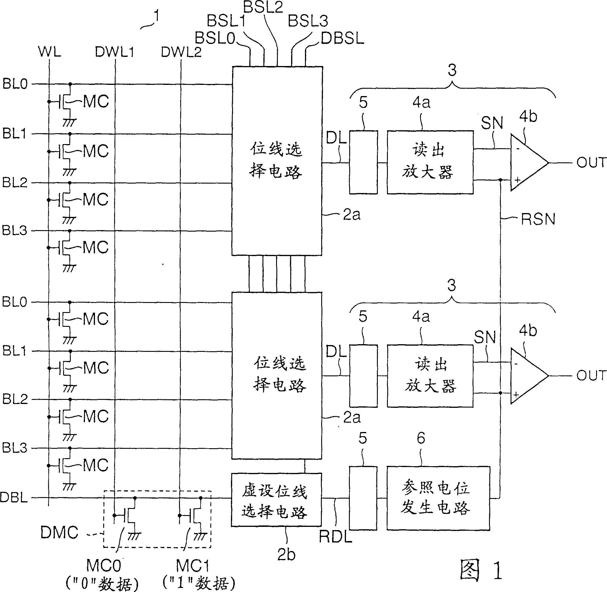
[0027] FIG. 1 shows the structure of a cell array 1 of a DRAM and a data readout circuit 3 connected thereto according to an embodiment of the present invention. DRAM cell MC consists of one MISFET with a floating channel body. Figure 4 The DRAM cell structure in the case of using an n-channel MISFET is shown in . A p-type silicon layer 12 isolated from the silicon substrate 10 by an insulating film 11 such as a silicon oxide film on a silicon substrate 10 is used as a channel body, has a gate electrode 14 formed through a gate insulating film 13, and serves as a source and a drain. n-type diffusion layers 15, 16.

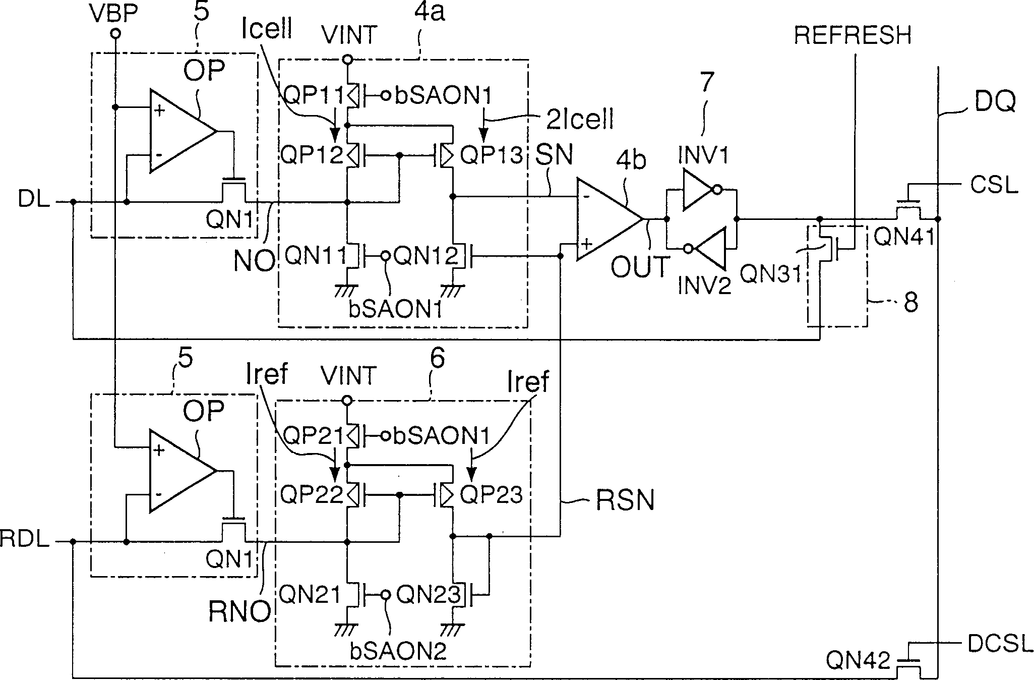
[0028] memory cell array 1 as Figure 5 constructed as shown in. That is, the DRAM cells MC have floating channel bodies that are isolated from other parts, and the source is used as a reference potential (ground potential). The drains of the DRAM cell...


PUM


Abstract

A semiconductor memory device has a memory cell array (1) including memory cells (MC); a reference current generating circuit (DMC) which generates a reference current (Iref); a reference voltage generating circuit (6) which generates a reference voltage in a reference node (RSN) on the basis of the reference current (Iref) generated by the reference current generating circuit; a first sense circuit (4a) which generates an output current (2Icell) on the basis of a cell current (Icell) of the selected memory cell and which generates a data potential in a sense node (SN) on the basis of the output current and the reference current; and a second sense circuit (4b) which detects the data held in the selected memory cell by comparing the data potential in the sense node with the reference voltage in the reference node.

Description

(1) Technical field [0001] The present invention relates to a semiconductor memory having a current sense type memory cell in which data is judged based on the presence or absence or magnitude of a cell current, and more particularly to a data readout circuit. (2) Background technology [0002] In conventional DRAMs, memory cells are formed using MISFETs and capacitors. With the adoption of the trench capacitor structure or stacked capacitor structure, the miniaturization of DRAM has made great progress, and the current unit cell size has been reduced to 8F with the minimum processing size as F. 2 area. However, it is becoming more and more difficult to ensure the same trend of cell size reduction as in the past. Here, there are technical difficulties in that the transistor must be made into a vertical transistor, the problem of increased interference between adjacent cells, and manufacturing technical difficulties such as processing and film formation. [0003] On the ot...

Claims


Application Information

Patent Timeline
Patent Type & Authority Patents(China)
IPC IPC(8): G11C11/40G11C11/4063H01L27/105G11C11/407G11C7/06
CPCG11C7/06G11C11/407
Inventor 藤田胜之大泽隆
Owner KK TOSHIBA
Why Eureka
Try Eureka