

Film magnetic storage device with data write-in by applying magnetic field
A storage device and data writing technology, applied in the direction of digital memory information, magnetic field controlled resistors, information storage, etc., can solve problems such as wrong data writing, achieve the effect of preventing data wrong writing and improving operation reliability
- Summary
- Abstract
- Description
- Claims
- Application Information
AI Technical Summary
Problems solved by technology
Method used
Image

Examples
Embodiment 1
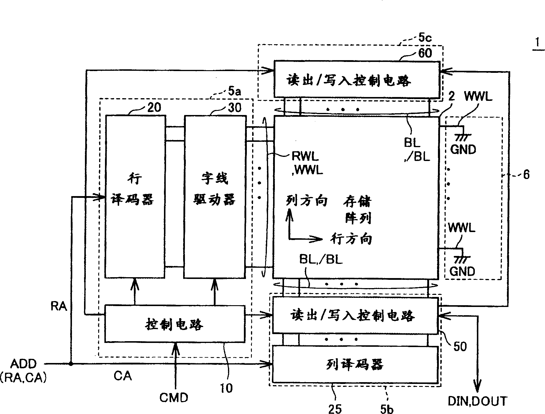
[0098] refer to figure 1 The MRAM device 1 of the embodiment of the present invention performs random access in response to an external control signal CMD and a signal line ADD, and performs input of read data DIN and output of read data DOUT.
[0099] The MRAM device 1 has a memory array 2 in which a plurality of MTJ memory cells are arranged in rows and columns, and peripheral circuits 5a, 5b, and 5c are arranged in the peripheral region of the memory array 2 in order to read and write data to the memory array 2. . In addition, hereinafter, the peripheral circuits 5a, 5b, and 5c are collectively referred to as the peripheral circuit 5 or the peripheral circuit 5#.
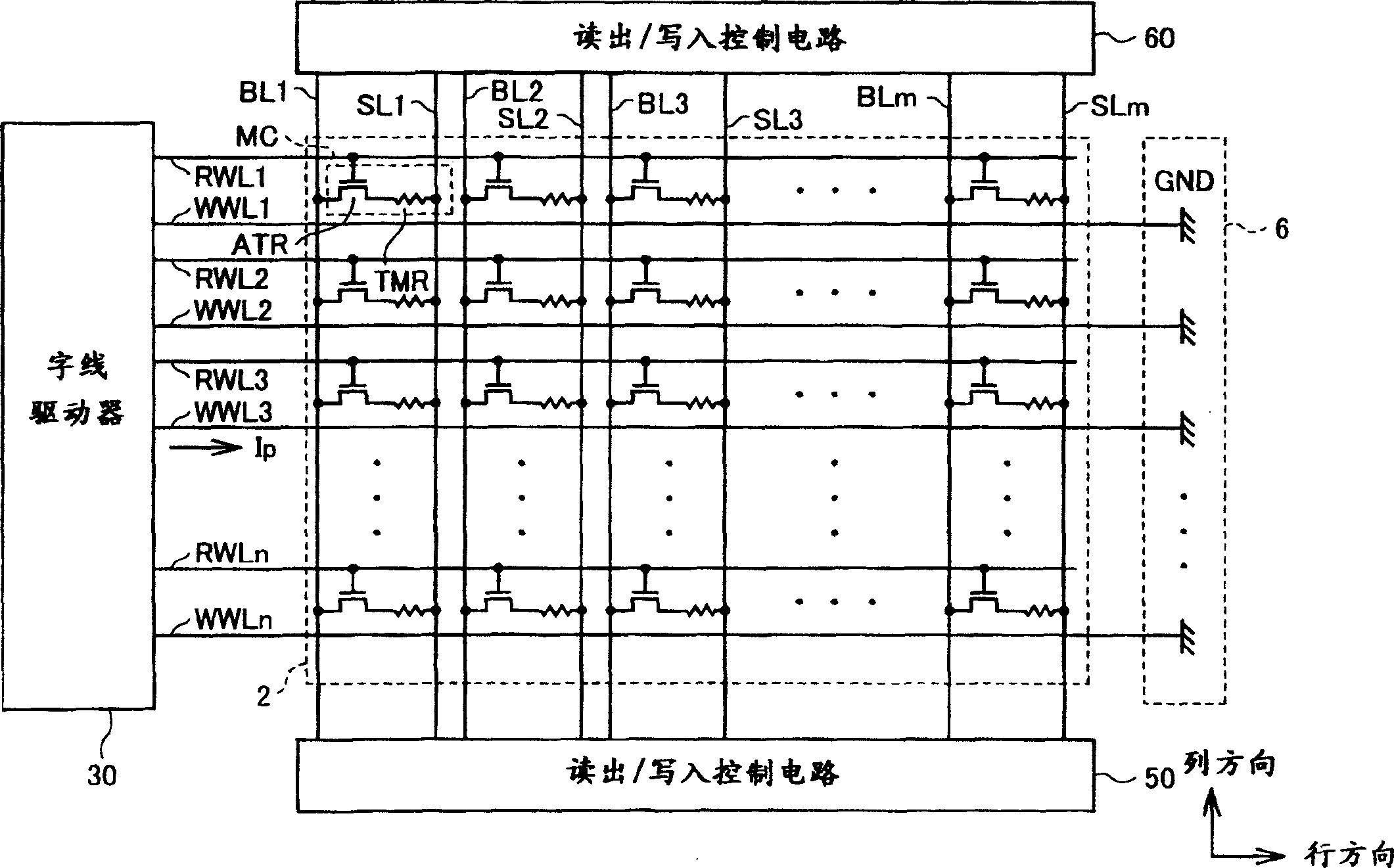
[0100] The structure of memory array 2 will be described in detail later, but a plurality of write word lines WWL and read word lines RWL are arranged corresponding to rows of MTJ memory cells (hereinafter also simply referred to as “memory cell rows”). In addition, bit lines BL are arranged corresponding to c...
Embodiment 2
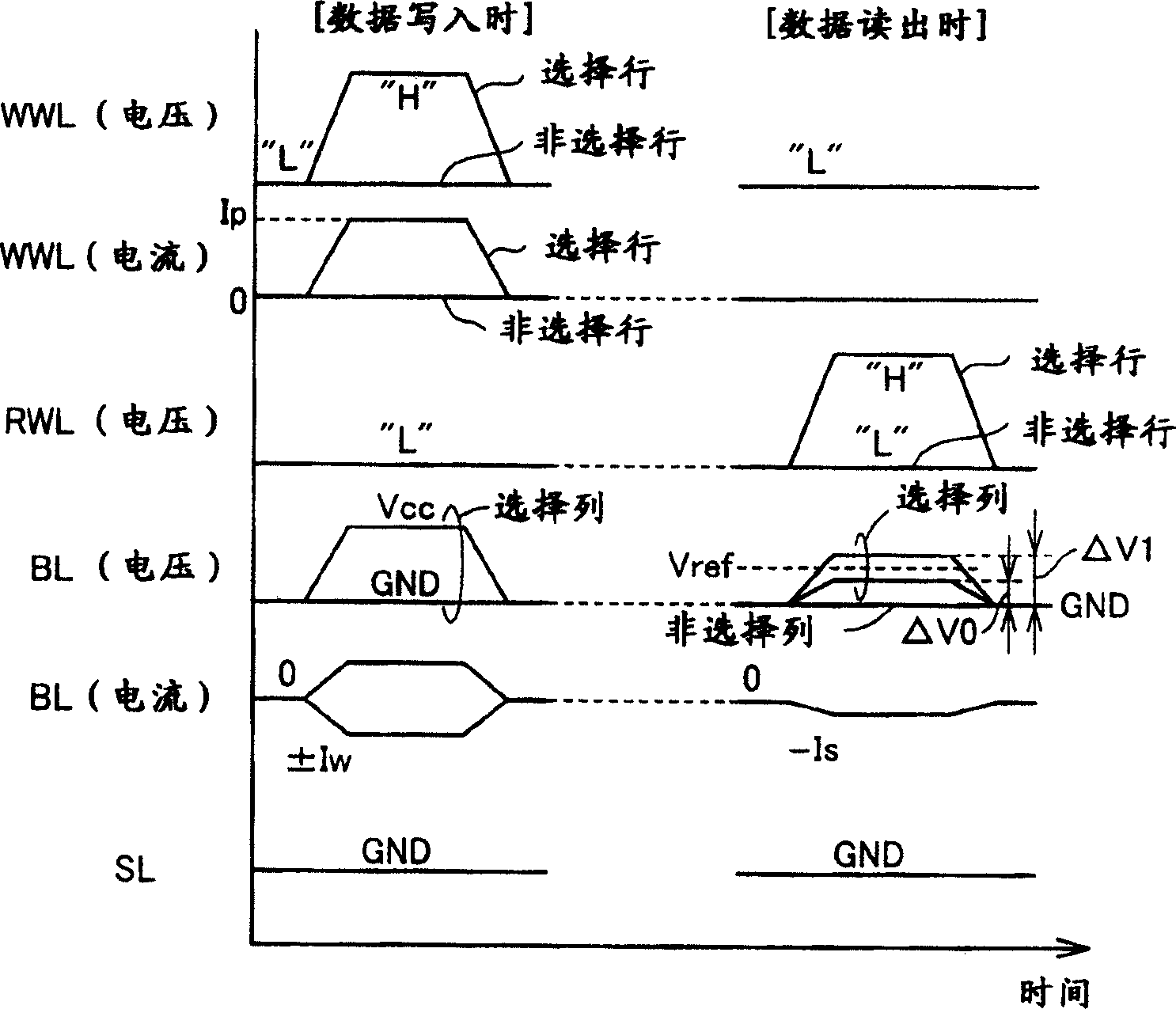
[0186] As explained in the item of the prior art, in the MRAM device, when data is written to the selected memory cell, for the non-selected memory cell belonging to the same memory cell row as the selected memory cell, only in the hard-to-magnetize axis In the (HA) direction, a predetermined data writing magnetic field is applied. Similarly, a predetermined data writing magnetic field is applied only to one side of the easy magnetization axis (EA) to an unselected memory cell belonging to the same memory cell column as the selected memory cell.
[0187] In each tunnel magnetoresistive element TMR, the free magnetization layer VL is magnetized in the direction corresponding to the level ("1" or "0") of the stored data along the easy axis (EA) direction, so it is most prone to error The non-selected memory cells in which the magnetization direction of the free magnetization layer VL is rewritten, that is, data is erroneously written, are memory cell groups associated with the s...
Embodiment 3
[0215] As described in the second embodiment, the magnetic noise from the power supply wiring becomes maximum when a peak current flows. Generally, for power supply wiring, decoupling capacitors are placed to suppress power supply fluctuations. A high-frequency current such as a peak current flowing through the power supply wiring passes through this decoupling capacitor. The decoupling capacitor occupies a relatively large area because it needs to have a certain amount of capacitor. Therefore, from the viewpoint of miniaturization and high integration of MRAM devices, it is important to efficiently arrange decoupling capacitors.
[0216] Figure 19 as well as Figure 20 It is a block diagram illustrating the first and second arrangement examples of decoupling capacitors in Embodiment 3, respectively.
[0217] refer to Figure 19 The power supply voltage lines PL are arranged, for example, along the column direction, and transmit the power supply voltage Vcc input to the ...
PUM
 Abstract
Description
Claims
Application Information