TFT array structure and manufacturing method thereof

An array structure and common electrode technology, applied in semiconductor/solid-state device manufacturing, instrumentation, optics, etc., can solve the problem of increasing the overlapping area of ​​gate electrode scanning lines and data lines and storage capacitors, and improving storage capacitors that cannot take into account the aperture ratio Optimize and increase the parasitic capacitance of the signal line to achieve the effect of increasing the storage capacitance, optimizing the design, and reducing the lead resistance

Inactive Publication Date: 2011-03-23
SHANGHAI TIANMA MICRO ELECTRONICS CO LTD
View PDF2 Cites 34 Cited by
  • Summary
  • Abstract
  • Description
  • Claims
  • Application Information

AI Technical Summary

Problems solved by technology

Although this method can better improve the aperture ratio, it is easy to cause point or line defects in the array on the one hand and increase the The parasitic capacitance on the signal line is reduced, and the delay phenomenon in signal transmission is aggravated
In addition, the lower electrode of the storage capacitor (that is, the gate electrode scanning line) is a light-shielding material, so it is impossible to take into account both the improvement of the aperture ratio and the optimization of the storage capacitor.

Method used


Image

  • TFT array structure and manufacturing method thereof
  • TFT array structure and manufacturing method thereof
  • TFT array structure and manufacturing method thereof

Examples


Embodiment Construction

[0054]In order to make the purpose and features of the present invention more comprehensible, the specific implementation manners of the present invention will be further described below in conjunction with the accompanying drawings.

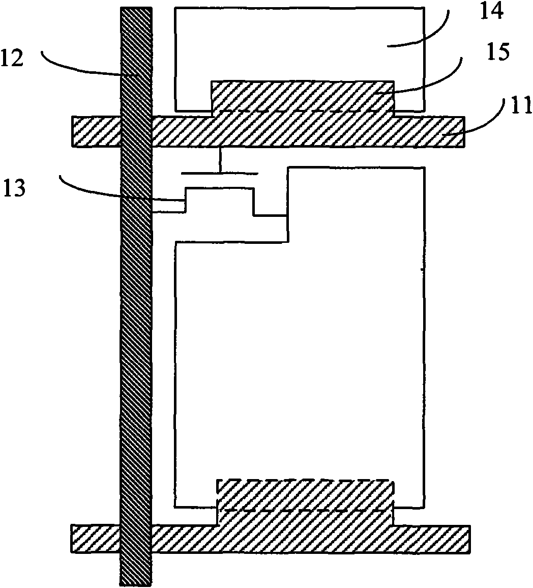
[0055] As mentioned in the background art, the lower electrode (ie, the common electrode) of the storage capacitor in the existing TFT array structure is made of a light-shielding material, so the two aspects of increasing the aperture ratio and optimizing the storage capacitor cannot be considered.
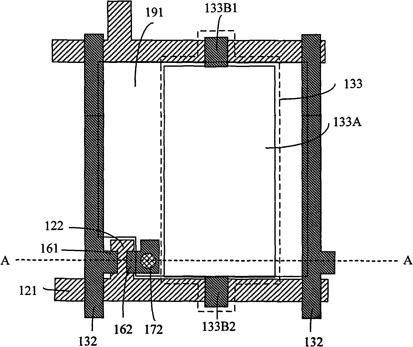
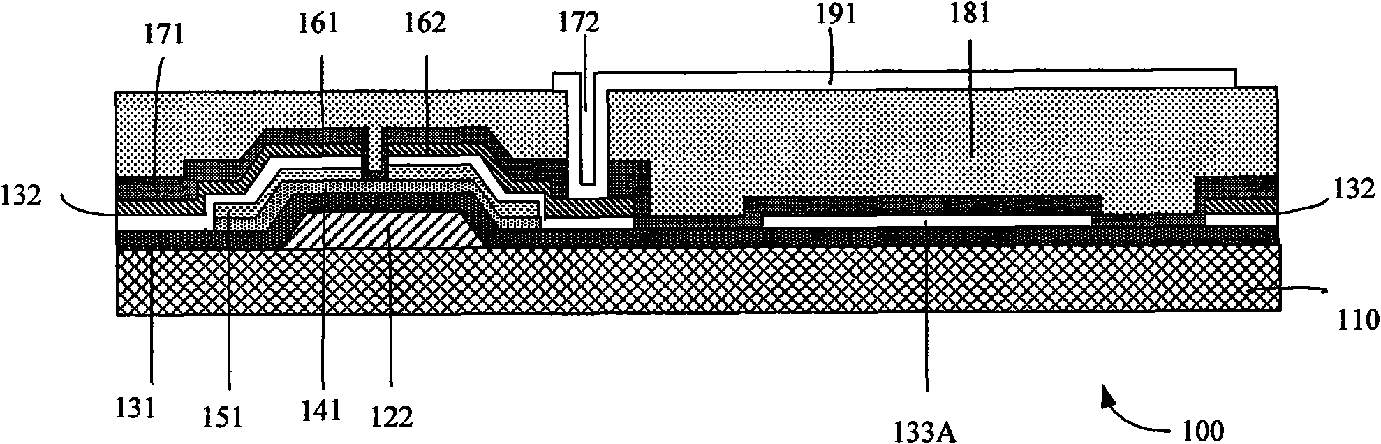
[0056] The core idea of ​​the present invention is to use a half-tone mask to form an at least partially transparent common electrode under the pixel electrode, thereby replacing the opaque common electrode and the pixel electrode with a transparent common electrode to form a storage capacitor structure, which can greatly improve the opening. At the same time, by increasing the width of the transparent common electrode, the storage capacitance can b...


PUM


Abstract

The invention discloses a thin film transistor (TFT) array structure and a manufacturing method thereof. The TFT array structure comprises a substrate, gate electrode scanning lines and a gate electrode integrated with the gate electrode scanning lines into a whole formed on the substrate, a gate electrode insulating layer formed on the gate electrode, a semiconductor active layer formed on the gate electrode insulating layer, data lines, a drain electrode and a source electrode integrated with the data lines formed on the gate electrode insulating layer, a common electrode formed on the gate electrode insulating layer, a passivation layer formed on the data lines, the drain electrode, the source electrode and the common electrode, and a pixel electrode formed on the passivation layer, wherein the drain electrode and the source electrode are partially lapped to the semiconductor active layer; a passivation via hole is formed on the drain electrode; the pixel electrode is connected with the drain electrode through the passivation layer via hole on the drain electrode; and the common electrode is at least made of a transparent material partially. The TFT array structure can improve the aperture opening ratio, optimize a storage capacitor and reduce lead resistance.

Description

technical field [0001] The invention relates to flat panel display technology, in particular to a thin film transistor (TFT) array structure and a manufacturing method thereof. Background technique [0002] With the focus on information display and the increasing demand for portable information media, research on flat panel display technology is flourishing. Among them, thin film transistor liquid crystal display (Thin Film Transistor Liquid Crystal Display, referred to as TFT-LCD) has the advantages of micro power consumption, low operating voltage, no X-ray radiation, high definition, small size, etc. In portable electronic products such as computers (Personal Digital Assistant, PDA). With the continuous increase of display screen size, resolution and display color types, achieving low power consumption and high brightness display is the main development direction of TFT-LCD at present, which puts higher demands on the structure and manufacturing process of TFT array. Re...

Claims


Application Information

Patent Timeline
IPC IPC(8): G02F1/1362G02F1/1368H01L21/82
Inventor 赵本刚袁剑峰李雄平马小军时伟强
Owner SHANGHAI TIANMA MICRO ELECTRONICS CO LTD
Why Eureka
Try Eureka