Film formation apparatus

A film-forming device and film-forming technology, applied in gaseous chemical plating, coating, photovoltaic power generation, etc., can solve problems such as joint leakage, influence of operation rate, and longer time required for decompression.

Active Publication Date: 2011-03-23
ULVAC INC
View PDF2 Cites 0 Cited by
  • Summary
  • Abstract
  • Description
  • Claims
  • Application Information

AI Technical Summary

Problems solved by technology

However, there is a limit to achieving high productivity when considering the installation area of ​​the device or cost-effectiveness
In addition, since the movement chamber and the film formation chamber need to be depressurized after joining the chamber, the time required for depressurization may become longer due to leakage from the junction.
In addition, since the number of moving chambers is smaller than the number of film forming chambers, the replacement time of the carriage may affect the operating rate of the entire device.

Method used


Image

  • Film formation apparatus
  • Film formation apparatus
  • Film formation apparatus

Examples


Embodiment Construction

[0088] according to Figure 1 to Figure 28 The thin-film solar cell manufacturing apparatus (film-forming apparatus) in the embodiment of the present invention will be described.

[0089] (thin film solar cell)

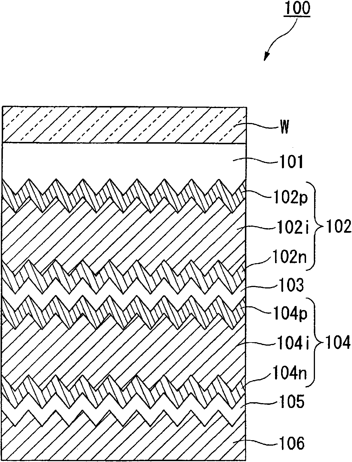
[0090] figure 1 This is a schematic cross-sectional view of a thin-film solar cell 100 manufactured by the thin-film solar cell manufacturing apparatus of the present invention.

[0091] Such as figure 1 As shown, a thin-film solar cell 100 is laminated with a substrate W made of glass constituting its surface, an upper electrode 101 made of a transparent conductive film arranged on the substrate W, a top cell 102 made of amorphous silicon, and a top cell 102 made of amorphous silicon. Between the top cell 102 and the bottom cell 104 described later are an intermediate electrode 103 made of a transparent conductive film, a bottom cell 104 made of microcrystalline silicon, a buffer layer 105 made of a transparent conductive film, and a back electrode 106 made of a m...


PUM


Abstract

The film formation apparatus includes a film formation chamber (11) that forms the desired film on a wafer (W) in vacuum, a loading and unloading chamber (13) that is fixed via a first opening and closing part (25) to said film formation chamber (11), which can be evacuated to form a vacuum state, a second opening and closing part (36) provided on the opposite face of said loading and unloading chamber (13) from where said first opening and closing part (25) is provided, and a carrier (21) that holds said wafer (W) so that the film formation surface of said wafer (W) is approximately parallelto the direction of gravity. Said carrier or said wafer (W) is loaded into and unloaded from said loading and unloading chamber (13) through said second opening and closing part (36). A plurality of said carriers (21) is arranged in parallel in said loading and unloading chamber (13). Said plurality of carriers (21) are loaded and unloaded in parallel between said loading and unloading chamber (13) and said film formation chamber (11), and films are formed simultaneously on said plurality of wafers (W) held on said plurality of carriers (21) in said film formation chamber (11).

Description

technical field [0001] The present invention relates to a film forming device. [0002] This application claims priority based on Japanese Patent Application No. 2008-149938 for which it applied on June 6, 2008, and uses the content here. Background technique [0003] Most of the materials used in current solar cells are monocrystalline Si-type and polycrystalline Si-type materials, and there are concerns about the shortage of Si materials. [0004] Therefore, in recent years, there has been an increasing demand for thin-film solar cells formed with a thin-film Si layer at low manufacturing costs and with little risk of material shortage. [0005] Furthermore, on the basis of existing thin-film solar cells having only the existing type a-Si (amorphous silicon) layer, conversion efficiency has recently been achieved by laminating an a-Si layer and a μc-Si (microcrystalline silicon) layer Demand for improved tandem thin film solar cells is rising. [0006] In the process of...

Claims


Application Information

Patent Timeline
Patent Type & Authority Applications(China)
IPC IPC(8): C23C16/54C23C16/24H01L31/04
CPCC23C16/24H01L21/67757C23C16/4587H01L21/67173H01L21/67754Y02E10/548H01L21/67712Y02E10/547C23C16/54H01L31/1804H01L21/67736H01L21/67161H01L31/076Y02P70/50
Inventor 清水康男小形英之松本浩一野口恭史若森让治冈山智彦森冈和杉山哲康重田贵司栗原広行
Owner ULVAC INC
Why Eureka
Try Eureka