Magnetron device

A magnetron and magnet technology, which is applied to magnetrons, discharge tubes, transit-time electron tubes, etc., can solve the problem of waste of magnetron sputtering equipment, etc. The effect of increasing usage

Active Publication Date: 2011-03-30
BEIJING NAURA MICROELECTRONICS EQUIP CO LTD
View PDF0 Cites 3 Cited by
  • Summary
  • Abstract
  • Description
  • Claims
  • Application Information

AI Technical Summary

Problems solved by technology

[0008] The problem solved by the present invention is how to avoid the waste of target material and improve the utilization rate of magnetron sputtering equipment

Method used


Image

  • Magnetron device
  • Magnetron device
  • Magnetron device

Examples


Embodiment 1

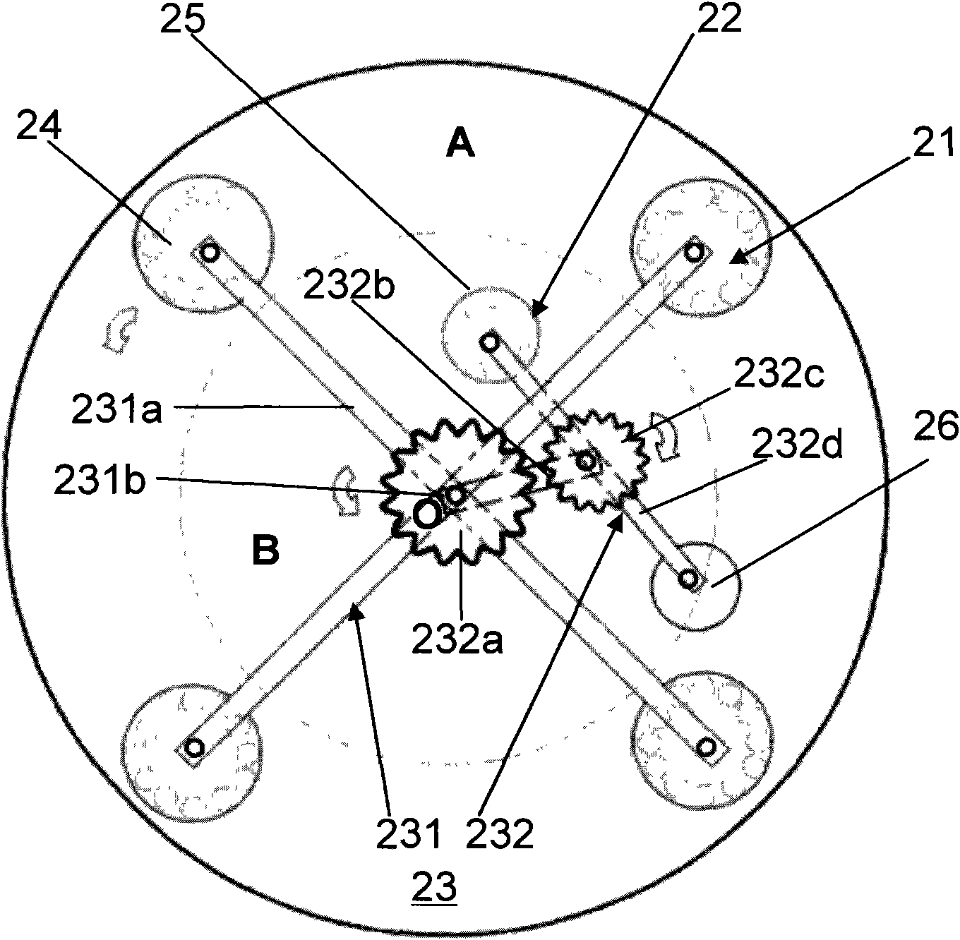
[0041] figure 2 It is a schematic structural diagram of the magnetron device described in this embodiment.

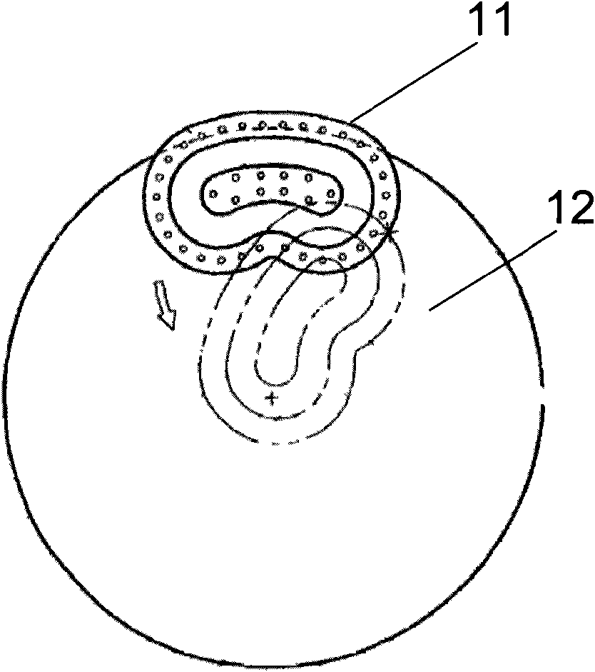
[0042]The magnetron device 20 is arranged on the side of the target material facing away from the vacuum chamber (not shown in the figure), and the target material is a commonly used circular metal target (the circle in the figure indicates the area occupied by the target material). The other side faces the semiconductor wafer to be processed in the vacuum chamber. The circular target includes an outer ring area A and a central area B inside the outer ring area A.

[0043] Such as figure 2 As shown, the magnetron device includes:

[0044] The outer ring area magnetron 21 is located in the outer ring area A;

[0045] The magnetron 22 in the central area is located in the central area B;

[0046] The rotating mechanism 23 is respectively connected with the magnetron 21 in the outer ring area and the magnetron 22 in the central area.

[0047] Wherein, the rotating ...

Embodiment 2

[0060] Figure 5 It is a schematic diagram of the structure of the magnetron device in this embodiment. In order to highlight the characteristics of the invention, the figure does not show the rotation mechanism in the outer ring area.

[0061] As shown in the figure, the difference from Embodiment 1 is that the outer ring area A is divided into two concentric sub-outer ring areas A1 and A2 with unequal radii, then the outer ring of the magnetron device described in this embodiment The zone magnetron 31 includes two corresponding sub-outer zone magnetrons 311 , 312 , wherein the sub-outer zone magnetron 311 is located inside the sub-outer zone magnetron 312 .

[0062] Similar to Embodiment 1, the magnetron in the sub-outer ring area includes at least one magnet group 34, and the magnet group 34 rotates synchronously with the center of the target as the rotating shaft, and the width of the magnet group in the two sub-outer ring area magnetrons The widths of the respective oute...


PUM


Abstract

The invention provides a magnetron device which is arranged at one side of a target, wherein, the target comprises an outer ring area and a central area positioned in the outer ring area. The magnetron device comprises an outer ring area magnetron positioned in the outer ring area, a central area magnetron positioned in the central area, and a rotating mechanism connected with the outer ring area magnetron and the central area magnetron respectively, wherein, the rotating mechanism drives the outer ring area magnetron to carry out circumferential rotation motion by taking the center of the target as a rotating shaft, and drive the central area magnetron to carry out circumferential rotation motion or asteroid track rotation motion by taking the center of the target as a rotating shaft. In the invention, the motion trail of the outer ring area magnetron covers the outer ring area of the target and meanwhile the motion trail of the central area magnetron covers the central area of the target so that magnetic force lines in a magnetic field are parallel or approximately parallel to the surface of the target can fully sweep through the whole area of the target, thus fully utilizing the material in the central part of the target and being beneficial to improving the utilization ratio of equipment.

Description

technical field [0001] The invention relates to the technical field of semiconductor processing, in particular to a magnetron device used in magnetron sputtering technology. Background technique [0002] As transistor dimensions continue to shrink to the sub-micron level, as predicted by Moore's Law, the number of transistors in high-efficiency, high-density integrated circuits rises to tens of millions. The signal integration of these huge number of active components requires more than ten layers of high-density metal wiring. However, the resistance and parasitic capacitance brought by these metal interconnections have become the main factors that limit the speed of this efficient integrated circuit. Driven by this factor, the semiconductor industry has developed from the original metal-aluminum interconnection process to metal-copper interconnection. At the same time, low dielectric constant dielectric materials have replaced silicon dioxide as the insulating medium betwee...

Claims


Application Information

Patent Timeline
Patent Type & Authority Applications(China)
IPC IPC(8): C23C14/35H01J25/50H01J23/02
Inventor 杨柏
Owner BEIJING NAURA MICROELECTRONICS EQUIP CO LTD
Why Eureka
Try Eureka