
Aligning and matching system and method for liquid crystal display panel

A liquid crystal display panel and the most matching technology, which is applied in the field of alignment matching system of liquid crystal display panels, can solve the problems of increasing production costs, deviations, and lowering the yield of liquid crystal display panels, so as to reduce defects and avoid circuit layout deviations. larger effect

Active Publication Date: 2012-07-25
KUSN INFOVISION OPTOELECTRONICS
View PDF0 Cites 0 Cited by
  • Summary
  • Abstract
  • Description
  • Claims
  • Application Information

AI Technical Summary

Problems solved by technology

However, due to the unavoidable existence of deviations between the circuit array (array) layout formed on the array substrate and the array layout on the array substrate in the ideal state in the prior art, and the differences between the circuits on the color filter substrate and the array substrate The layout of the color filter or color filter circuit corresponding to the array (referred to as CF layout) also has the defect of deviation from the CF layout on the ideal CF substrate. Therefore, in the alignment of the liquid crystal display panel , In the bonding process, there will also inevitably be layout deviations between the array substrate and the color filter substrate. However, if the deviation between the array layout on the array substrate and the ideal state is the same as the CF layout on the color filter substrate When the deviation from the ideal state is too large, and the gap between the two is not found until after the array substrate and the color filter substrate are bonded, the defects of the liquid crystal display panel caused by this time have not been improved. Therefore, it will inevitably lead to a reduction in the manufacturing yield of liquid crystal display panels, thereby increasing production costs

Method used


Image

  • Aligning and matching system and method for liquid crystal display panel
  • Aligning and matching system and method for liquid crystal display panel
  • Aligning and matching system and method for liquid crystal display panel

Examples


Embodiment Construction

[0025] In order to make the purpose, technical solutions and beneficial effects of the present invention more clearly, the present invention will be further described in detail below in conjunction with the accompanying drawings and specific embodiments.

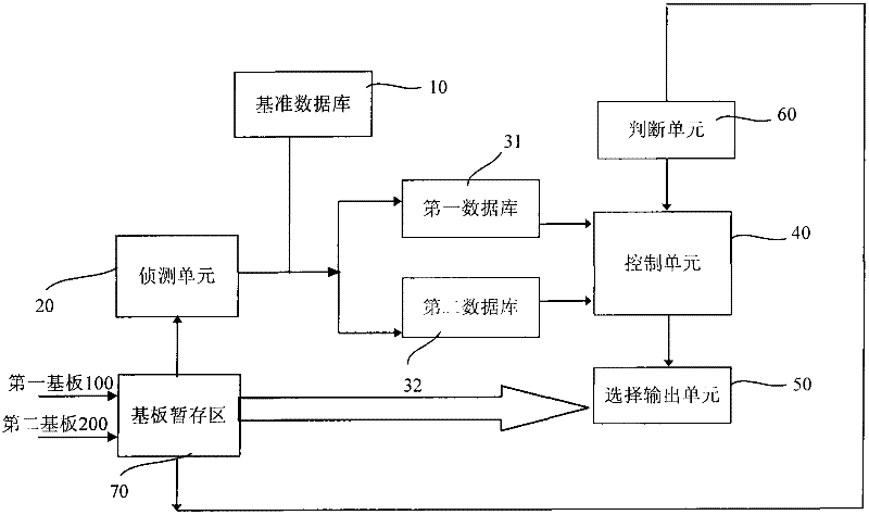
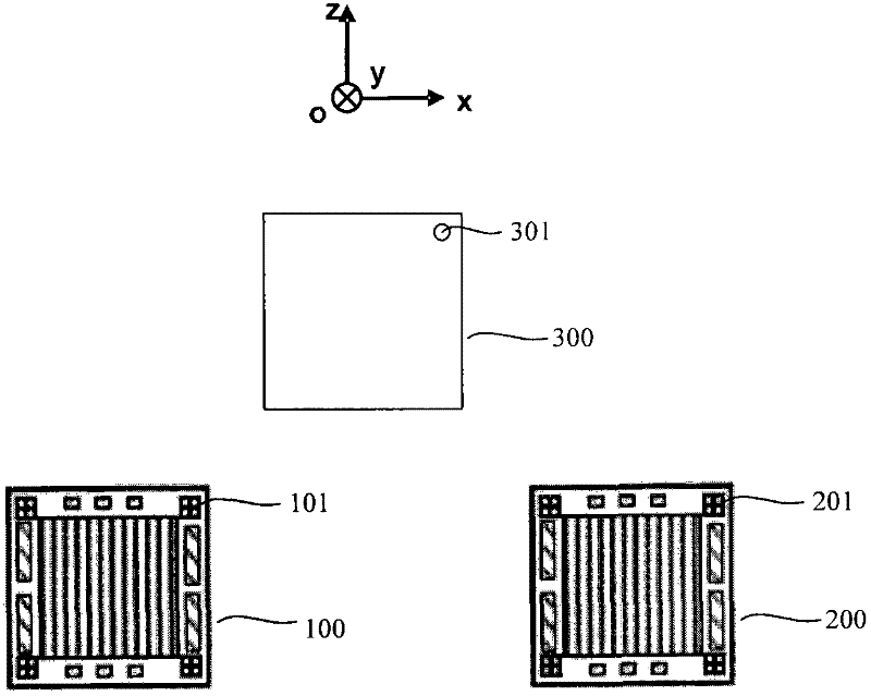
[0026] The invention provides an alignment matching system of a liquid crystal display panel, which firstly combines image 3 refer to figure 2 ,in, figure 2 It is a block diagram of an alignment matching system of a liquid crystal display panel in a preferred embodiment of the present invention, image 3 It is a schematic diagram of the alignment matching of the liquid crystal display panel in the embodiment of the present invention. The liquid crystal display panel includes a first substrate 100 and a second substrate 200 facing each other, wherein the first substrate 100 has a first plane coordinate mark 101 for alignment, and the second substrate 200 has a second plane coordinate mark 101 for alignment. ID 201. In ...


PUM


Abstract

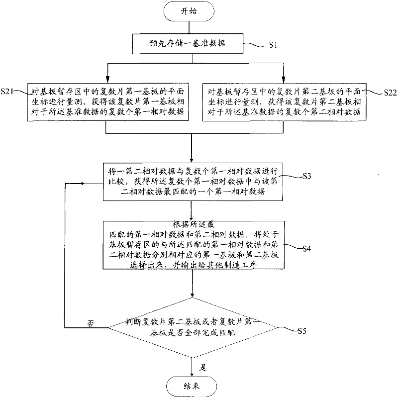
The invention provides an aligning and matching system for a liquid crystal display panel. The system comprises a substrate temporary storage region, a reference database, a detection unit, a first database, a second database, a control unit and a selection and output unit, wherein the detection unit measures first relative data and second relative data, relative to reference data in the reference database, of the first substrate and the second substrate in the liquid crystal display panel; the control unit matches the first relative data with the second relative data and acquires the first relative data and the second relative data which are matched with each other best; and the selection and output unit selects the first substrate and the second substrate, respectively corresponding to the first relative data and the second relative data which are matched with each other best, in the substrate temporary storage region according to the first relative data and the second relative datawhich are matched with each other best, and outputs the selected first substrate and the selected second substrate to other manufacturing processes. The invention also provides an aligning and matching method for the liquid crystal display panel. By using the system and the method, the alignment accuracy of the first substrate and the second substrate of the liquid crystal display panel are improved.

Description

technical field [0001] The invention relates to the technical field of liquid crystal display, in particular to a system and method for alignment matching of a liquid crystal display panel. Background technique [0002] Since thin film transistor liquid crystal display (TFT LCD: Thin Film Transistor Liquid Crystal Display) has the advantages of small size, light weight, low radiation, etc., thin film transistor liquid crystal display has been widely used in various electronic devices, and is becoming more and more Loved by many users. With the continuous improvement of liquid crystal display manufacturing technology, how to manufacture thin film transistor liquid crystal displays at a lower cost has become one of the technical development trends in this field. [0003] A display panel of a thin film transistor liquid crystal display generally includes: an array substrate, a color filter (CF) substrate, and a liquid crystal layer sealed between the array substrate and the co...

Claims


Application Information

Patent Timeline
Patent Type & Authority Patents(China)
IPC IPC(8): G02F1/1333
Inventor 朱健
Owner KUSN INFOVISION OPTOELECTRONICS
Learn More