Palladium/carbon/silicon heterojunction material with hydrogen sensitive effect

A technology of silicon heterojunction and hydrogen, applied in the direction of material resistance, material capacitance, etc., can solve the problems of complex sensor preparation process, detection of hydrogen, and the electrical characteristics of palladium film/carbon film/silicon heterojunction materials, etc., to achieve High sensitivity, short response time and good stability

Inactive Publication Date: 2011-04-13
CHINA UNIV OF PETROLEUM (EAST CHINA)
View PDF2 Cites 12 Cited by
  • Summary
  • Abstract
  • Description
  • Claims
  • Application Information

AI Technical Summary

Problems solved by technology

The hydrogen gas sensitivity of nano-oxides usually has a good effect at high temperature, and the preparation process of sensors based on nanowires or nanotubes is complicated
[0004] At present, there is no report of using the electrical properties of palladium film / carbon film / silicon heterojunction materials to detect hydrogen

Method used


Image

  • Palladium/carbon/silicon heterojunction material with hydrogen sensitive effect
  • Palladium/carbon/silicon heterojunction material with hydrogen sensitive effect
  • Palladium/carbon/silicon heterojunction material with hydrogen sensitive effect

Examples


Embodiment 1

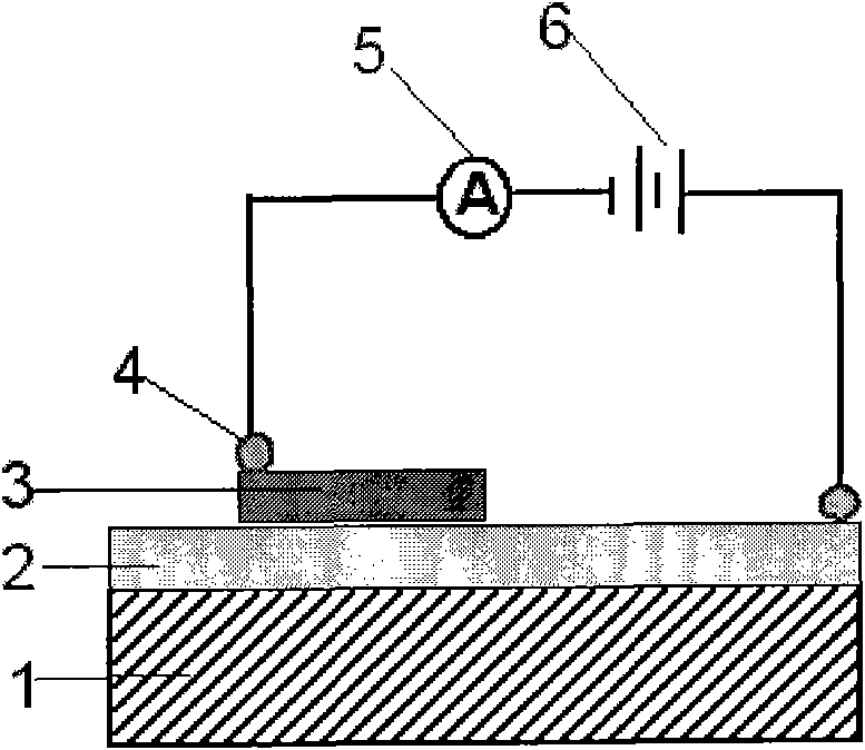
[0022] Example 1, take graphite powder with a mass concentration of 99.9% and make a pure graphite target by cold pressing. Use magnetron sputtering method to sputter pure graphite target to an area of ​​0.8cm 2 , a thickness of 0.5 to 1.0 mm on a monocrystalline silicon substrate 1, on the monocrystalline silicon substrate, a carbon film 2 with a thickness of about 100 nanometers is formed, and then the mass concentration is 99.9% by magnetron sputtering. % of the palladium target is sputtered onto the carbon film 2, forming a 0.3cm area on the surface of the carbon film 2 2 , a palladium film 3 with a thickness of 20nm, connect a DC power supply 6 on the heterojunction material, such as figure 1 As shown, among the figure 4 is the contact point of power line and material, 5 is an ammeter, becomes the conductivity type hydrogen gas sensor. The preparation parameters of the heterojunction material: ① pure carbon film: the sputtering DC voltage is 0.40 kV, the sputtering DC c...

Embodiment 2

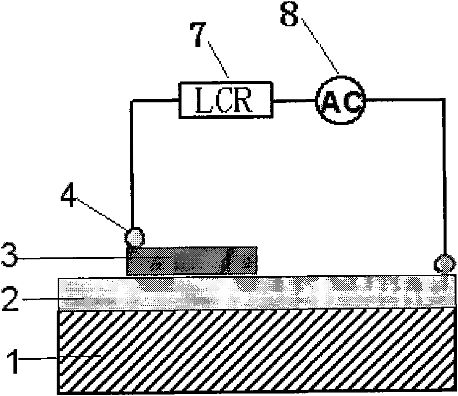
[0024] Example 2, take graphite powder with a purity of 99.9% and make a pure graphite target by cold pressing. Use magnetron sputtering method to sputter pure graphite target to an area of ​​0.8cm 2 , a thickness of 0.5 to 1.0 mm on a monocrystalline silicon substrate 1, on the monocrystalline silicon substrate, a carbon film 2 with a thickness of about 100 nanometers is formed, and then the mass concentration is 99.9% by magnetron sputtering. % of the palladium target is sputtered onto the carbon film 2, forming a 0.3cm area on the surface of the pure carbon film 2 2 , a palladium film 3 with a thickness of 20nm, such as figure 2 As shown, 8 in the figure is the AC signal loaded by the heterojunction material, 4 is the contact point between the power line and the material, and 7 is the precision LCR digital bridge, which becomes a capacitive hydrogen gas sensor. The preparation parameters of the heterojunction material: ① pure carbon film: the sputtering DC voltage is 0.4...


PUM

PropertyMeasurementUnit
thicknessaaaaaaaaaa
thicknessaaaaaaaaaa
thicknessaaaaaaaaaa

Abstract

The invention provides a palladium film / carbon film / silicon heterojunction material with hydrogen sensitive effect. The material is made by the steps of: sputtering 99.9% graphite palladium on a polished silicon substrate by using a magnetron sputtering method to form a carbon film with 20-20 nm in thickness; and then sputtering a pure palladium film which is 10-30 nm in thickness on the pure carbon film. The palladium film / carbon film / silicon heterojunction material has obvious hydrogen sensitive effect and can be used for preparing a conductive or capacitive hydrogen sensitive sensor. The material works at room temperature and is easy to prepare, the miniaturization and the integration of a device are easy to realize, and the material has high sensitivity, short response time, good stability, simple production process, low cost and broad application prospect.

Description

technical field [0001] The invention relates to a new material with hydrogen sensitive effect, which is used for making gas sensitive sensor. Background technique [0002] Hydrogen is the main industrial raw material and the most important industrial and specialty gas. Hydrogen energy is an important secondary energy source. When the volume of hydrogen contained in the air accounts for 4% of the mixed volume, it will explode when it is ignited. At present, most hydrogen sensors are made of metal oxides (such as tungsten, tin, zinc oxides, etc.), doped carbon nanotubes and graphene, oxides and rare metals (palladium, platinum), etc. become. The preparation process of metal oxides is relatively complicated, and often requires solution reaction at low temperature, drying, calcination at medium temperature, calcination at high temperature, aging and other processes. The whole process takes dozens of days, and some metal oxides are harmful to the human body. Doped carbon nano...

Claims


Application Information

Patent Timeline
Patent Type & Authority Applications(China)
IPC IPC(8): G01N27/04G01N27/22
Inventor 薛庆忠李建鹏陈惠娟马明周小岩王盛
Owner CHINA UNIV OF PETROLEUM (EAST CHINA)
Why Eureka
Try Eureka