Palladium/carbon/silicon heterojunction material with hydrogen sensitive effect
A silicon heterojunction and hydrogen technology, applied in the direction of material resistance, material capacitance, etc., can solve the problems of detecting hydrogen, not using palladium film/carbon film/silicon heterojunction material electrical characteristics, complex sensor preparation process, etc., to achieve Short response time, high sensitivity and good stability
- Summary
- Abstract
- Description
- Claims
- Application Information
AI Technical Summary
Problems solved by technology
Method used
Image
Examples
Embodiment 1
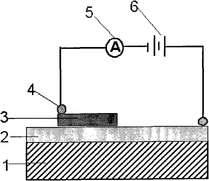
[0022] Example 1, take graphite powder with a mass concentration of 99.9% and make a pure graphite target by cold pressing. Use magnetron sputtering method to sputter pure graphite target to an area of 0.8cm 2 , a thickness of 0.5 to 1.0 mm on a monocrystalline silicon substrate 1, on the monocrystalline silicon substrate, a carbon film 2 with a thickness of about 100 nanometers is formed, and then the mass concentration is 99.9% by magnetron sputtering. % of the palladium target is sputtered onto the carbon film 2, forming a 0.3cm area on the surface of the carbon film 2 2 , a palladium film 3 with a thickness of 20nm, connect a DC power supply 6 on the heterojunction material, such as figure 1 As shown, among the figure 4 is the contact point of power line and material, 5 is an ammeter, becomes the conductivity type hydrogen gas sensor. The preparation parameters of the heterojunction material: ① pure carbon film: the sputtering DC voltage is 0.40 kV, the sputtering DC c...
Embodiment 2
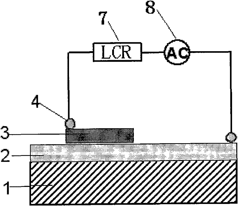
[0024] Example 2, take graphite powder with a purity of 99.9% and make a pure graphite target by cold pressing. Use magnetron sputtering method to sputter pure graphite target to an area of 0.8cm 2 , a thickness of 0.5 to 1.0 mm on a monocrystalline silicon substrate 1, on the monocrystalline silicon substrate, a carbon film 2 with a thickness of about 100 nanometers is formed, and then the mass concentration is 99.9% by magnetron sputtering. % of the palladium target is sputtered onto the carbon film 2, forming a 0.3cm area on the surface of the pure carbon film 2 2 , a palladium film 3 with a thickness of 20nm, such as figure 2 As shown, 8 in the figure is the AC signal loaded by the heterojunction material, 4 is the contact point between the power line and the material, and 7 is the precision LCR digital bridge, which becomes a capacitive hydrogen gas sensor. The preparation parameters of the heterojunction material: ① pure carbon film: the sputtering DC voltage is 0.4...
PUM
| Property | Measurement | Unit |
|---|---|---|
| thickness | aaaaa | aaaaa |
| thickness | aaaaa | aaaaa |
| thickness | aaaaa | aaaaa |
Abstract
Description
Claims
Application Information


