Clock switching method and device

A clock switching and clock domain technology, applied in the direction of generating/distributing signals, logic circuits using basic logic circuit components, logic circuits using specific components, etc., can solve problems such as logical confusion, complex operation, and gating output glitches. To achieve the effect of ensuring stability, excellent characteristics, and smooth switching

Active Publication Date: 2011-04-13
HISENSE VISUAL TECH CO LTD
View PDF8 Cites 24 Cited by
  • Summary
  • Abstract
  • Description
  • Claims
  • Application Information

AI Technical Summary

Problems solved by technology

For example, the Chinese utility model CN2872451Y discloses a new type of clock dynamic switching circuit. Although the problem of metastable state is solved to a certain extent, when the frequency difference between the fast and slow clocks is large, it is difficult to avoid the glitch phenomenon caused by the superimposition of the gate control output.
Invention patent CN100587652C discloses a clock switching method and a clock switching device. There are many steps and complicated operation, and it must be known in advance which of the two clock signals to be switched is which clock is faster and which clock is slow. The fast and slow clock signals must be The smooth switching of the clock signal can only be achieved by inputting to a specific port, so the actual application situation is not ideal
After logic simulation, we found that when the clock selection signal clk_sel changes near the rising edge of clk1 or clk2, the patented technology is not perfect for the metastable state, which may easily lead to logic confusion

Method used


Image

  • Clock switching method and device
  • Clock switching method and device
  • Clock switching method and device

Examples


Embodiment 1

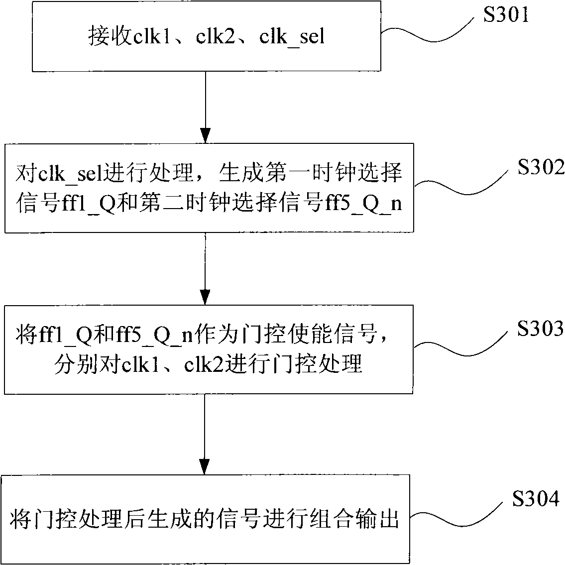
[0044] Embodiment 1, this embodiment proposes a clock switching method, see image 3 shown, including the following steps:

[0045] S301. Receive a first clock signal clk1, a second clock signal clk2, and a clock selection signal clk_sel for switching and outputting the clk1 and clk2.

[0046] S302. Process the clock selection signal clk_sel to generate a first clock selection signal ff1_Q and a second clock selection signal ff5_Q_n.

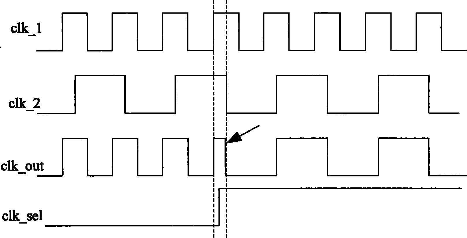
[0047] Among them, ff1_Q is used for enabling control of clk1, and ff5_Q_n is used for enabling control of clk2. When clk_sel is in the state of selecting clk1 output, ff1_Q enters the state of gating clk1 output, and ff5_Q_n enters the state of blocking clk2 output; when clk_sel is in the state of selecting clk2 output, ff1_Q enters the state of blocking clk1 output, and ff5_Q_n enters the state of gating clk2 the state of the output. When clk_sel jumps, in order to avoid glitches or metastable problems in the output clock signal, it is nece...

Embodiment 2

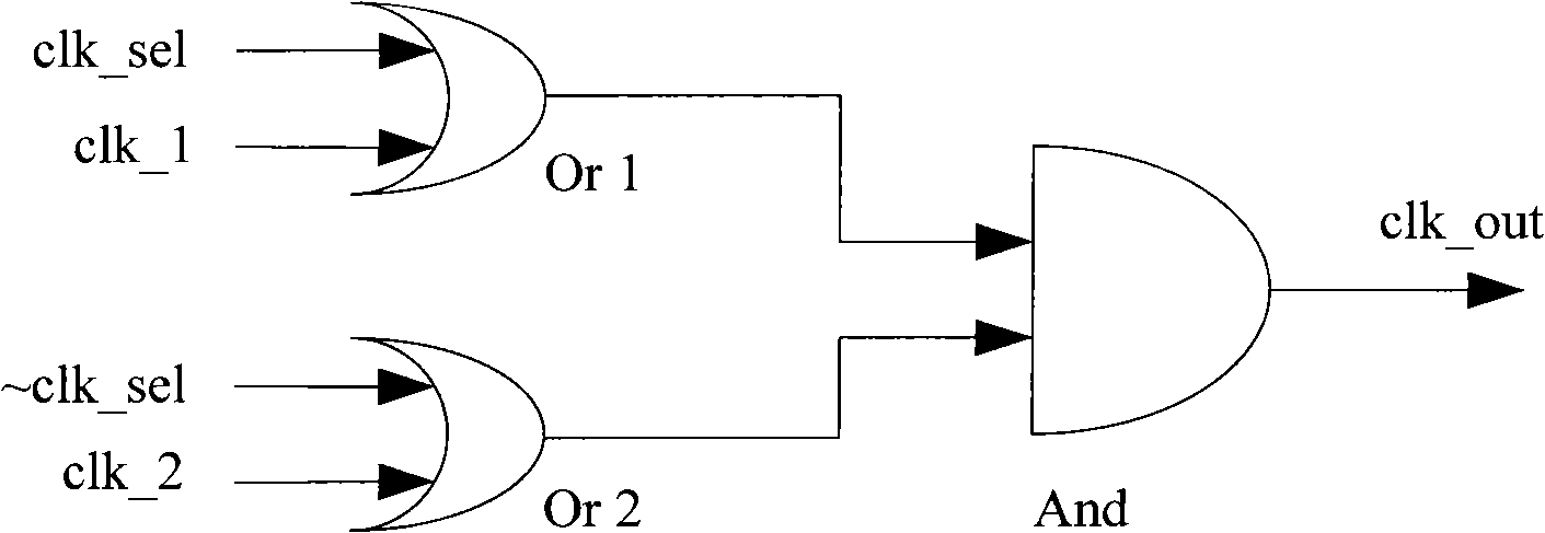
[0059] Embodiment 2, this embodiment is a hardware circuit architecture diagram proposed to implement the clock switching method described in Embodiment 1, see Image 6 As shown, it includes four groups of D flip-flops D1-D4, a first clock gating processing module U1, a second clock gating processing module U2 and a combined processing module U3. Among them, the first and fourth groups of D flip-flops D1 and D4 work in the first clock domain, that is, their clock terminal CP receives the first clock signal clk1; the second and third groups of D flip-flops D2 and D3 work in the first clock domain The second clock domain, that is, its clock terminal CP receives the second clock signal clk2. The clock selection signal clk_sel output by the system for switching clk1 and clk2 is transmitted to the data terminals D of the first and third groups of D flip-flops D1 and D3 respectively, and is synchronously processed by the first group of D flip-flops D1 to generate the first clock sel...


PUM


Abstract

The invention discloses a clock switching method and device. The method comprises the following steps: firstly processing a clock selection signal to generate a first clock selection signal and a second clock selection signal, wherein when the clock selection signal transfers into a strobe clk2 state from a strobe clk1 state, the first clock selection signal transfers at the time of keeping at least one clk1 impulse of the strobe clk1 state; and the second clock selection signal transfers at the time of keeping at least two clk2 impulses of the existing blocking-up clk2 state after the first clock selection signal transfers; then taking the first and second clock selection signals as gating enable signals so as to respectively perform gating processing on the clk1 and the clk2; and finally outputting signals generated by the gating processing in a combination mode. In the invention, although the clock selection signals change at any time, burrs of an output clock do not generate, thus realizing smooth switching among clocks with any frequencies.

Description

technical field [0001] The invention belongs to the technical field of clock signal processing, and in particular relates to a clock signal switching method and a clock switching device. Background technique [0002] In the digital video processing chip, according to the needs of the application, it is often necessary to switch the input clock. For example: a video processing chip has two input clocks clk1 and clk2. When the video stream input to the video processing chip is at low resolution, the working clock of the chip is required to be clk1; when the video stream input to the video processing chip works at For high resolution, the working clock of the chip is required to be clk2. [0003] The switching time of the two input clocks clk1 and clk2 is completely unknown to this video processing chip. If no special processing is done, a selector is directly used to select one of the clock signal outputs, which may make the circuit of this video processing chip An unknown p...

Claims


Application Information

Patent Timeline
Patent Type & Authority Applications(China)
IPC IPC(8): G06F1/08H03K19/173
Inventor 聂中平
Owner HISENSE VISUAL TECH CO LTD
Why Eureka
Try Eureka