

Forming method of diffusion zone
A diffusion area and pre-doping technology, which is applied in the direction of electrical components, semiconductor/solid-state device manufacturing, circuits, etc., can solve the problems of uneven ion implantation, lattice damage, and increased production costs, and achieve uniform distribution of impurity ions, Improved crystal structure and improved production cost
- Summary
- Abstract
- Description
- Claims
- Application Information
AI Technical Summary
Problems solved by technology
Method used
Image

Examples
no. 1 example
[0046] In order to characterize the doping of the buried layer region, the sheet resistance of the obtained N-type buried layer was measured by the four-probe method. In this embodiment, the measured Rs result was 140Ω / □, and the measured diffusion depth was 0.7 μm. The above is the content of the first embodiment of the present invention.
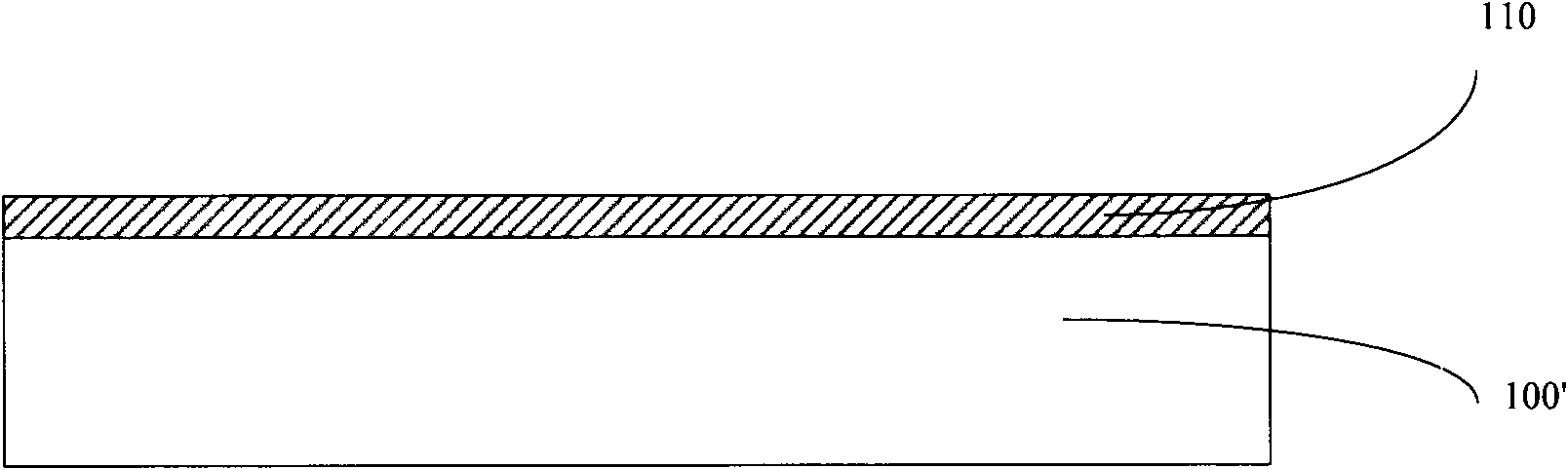
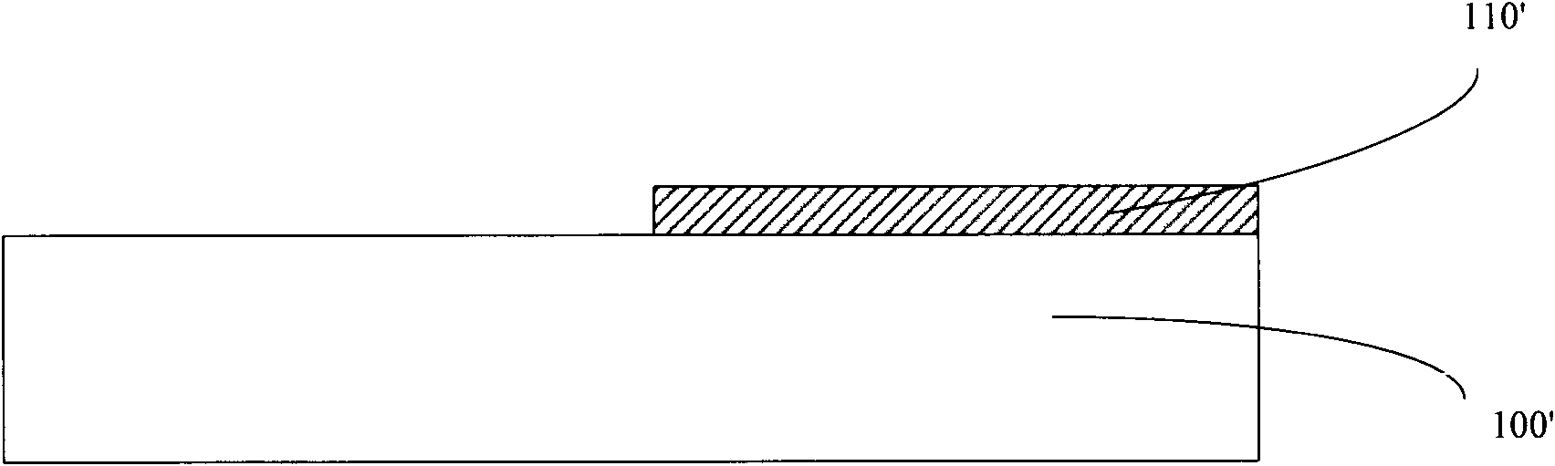
[0047] Due to the limitation of the saturated vapor pressure of TEASAT and the toxicity of the substance, for safety reasons, the As content in the pre-doped layer 310' is below a certain dose, and thus the content of As diffused into the semiconductor substrate 300 is also limited, resulting in The formed N-type buried layer has low doping rate and high resistivity. In this case, it is often necessary to achieve the corresponding resistivity requirements through multiple diffusions. The flow process of the second embodiment of the present invention is as follows Figure 8 As shown, a higher concentration of As doping in the N-type burie...
PUM
| Property | Measurement | Unit |
|---|---|---|
| electrical resistivity | aaaaa | aaaaa |
Abstract
Description
Claims
Application Information