Non-volatile semiconductor memory device
A storage device, non-volatile technology, used in semiconductor devices, semiconductor/solid-state device manufacturing, transistors, etc., can solve problems such as high cost, reduce memory cell integration, and reduce area and power consumption. , the effect of high integration
- Summary
- Abstract
- Description
- Claims
- Application Information
AI Technical Summary
Problems solved by technology
Method used
Image
Examples
Embodiment 1
[0054] The nonvolatile semiconductor memory device of this embodiment includes a plurality of memory cells (basic cells for storing data), a plurality of source lines, a plurality of bit lines, and a plurality of word lines arranged in a matrix. Each of the memory cells includes a storage element electrically connected to one of the source lines, one of the bit lines, and one of the word lines. In this embodiment, memory transistors are used as memory elements.
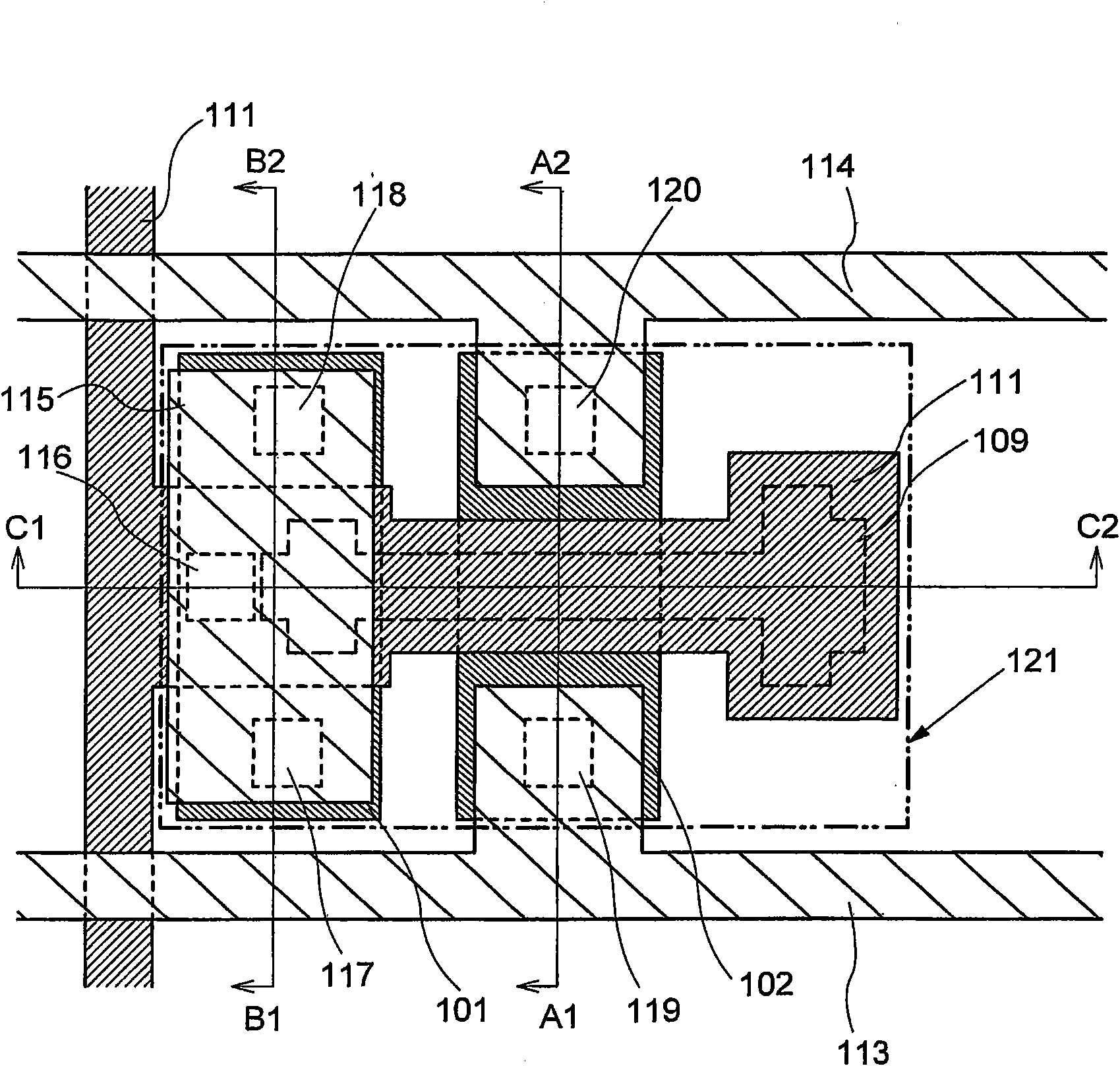
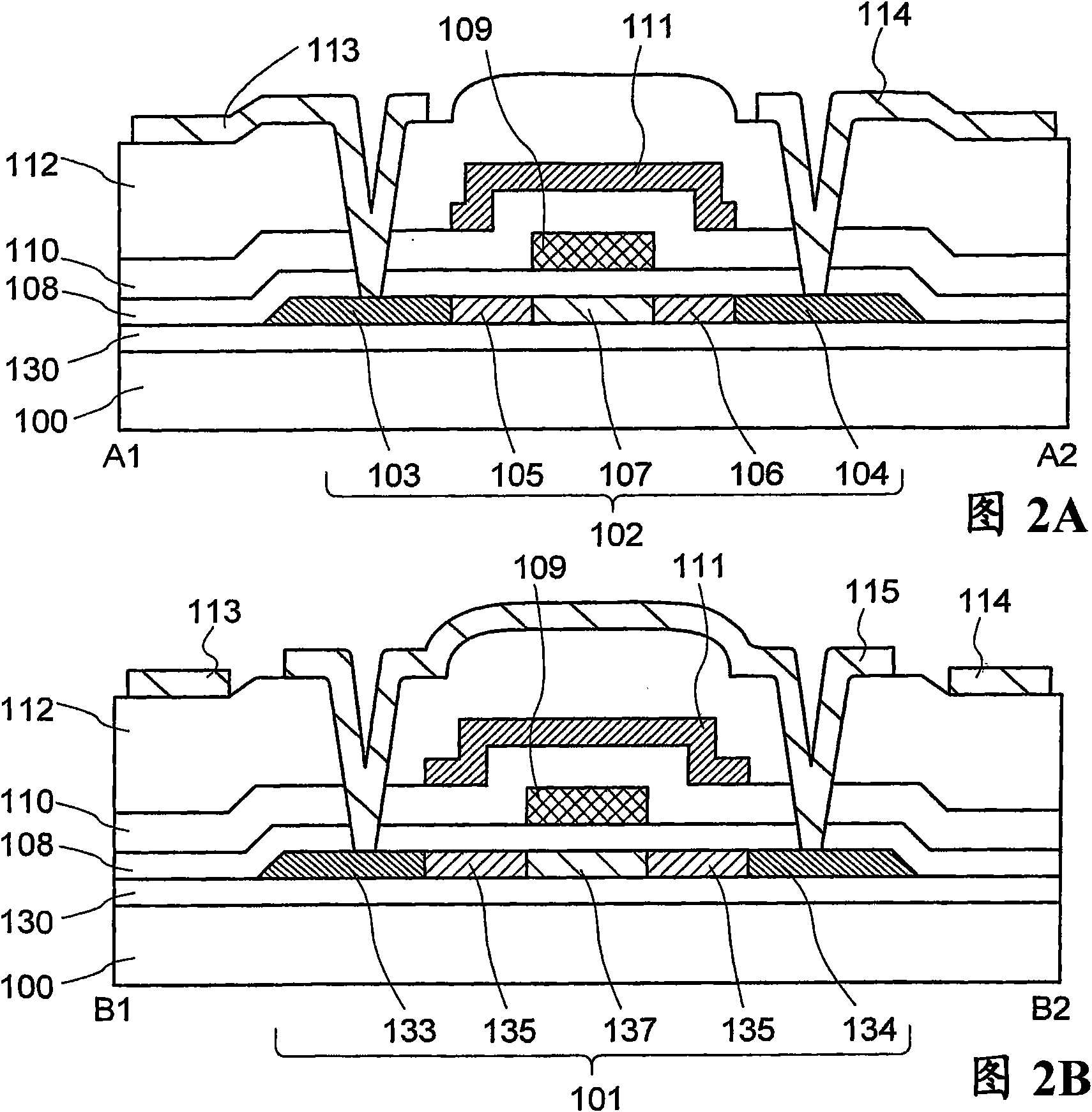
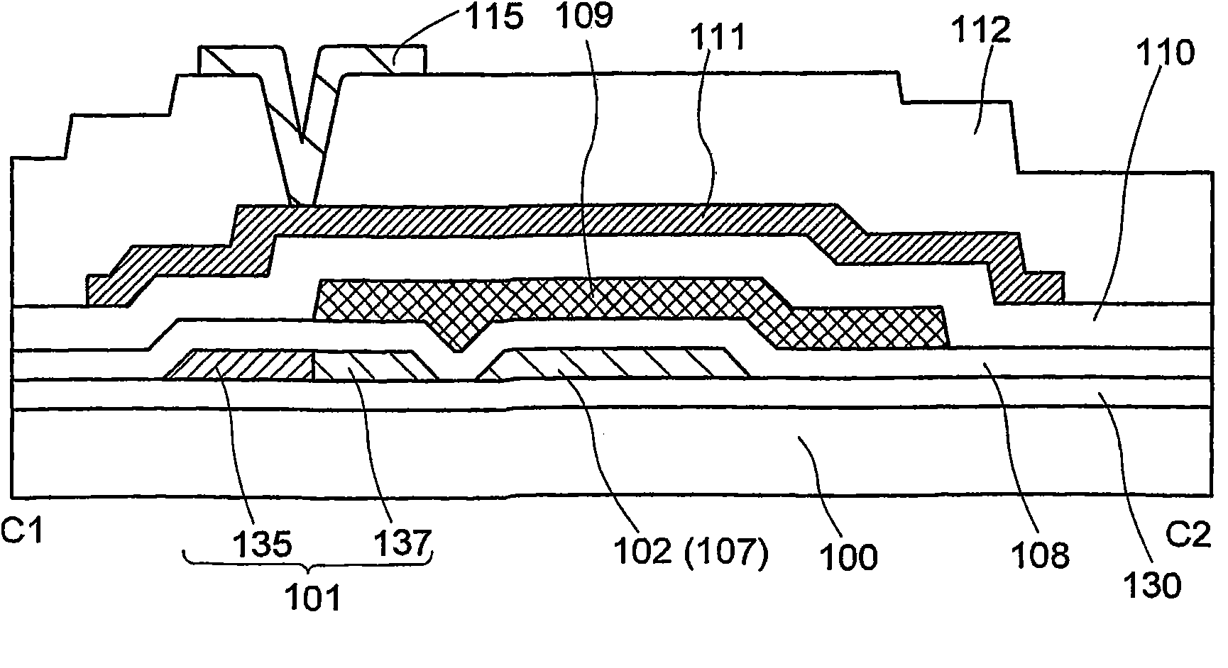
[0055] will refer to figure 1 , Figure 2A to Figure 2C , image 3 and Figure 4 A nonvolatile semiconductor memory device (hereinafter also referred to as a memory device) of this embodiment will be described. figure 1 is a plan view showing the layout of one memory cell of the memory device in this embodiment. Figure 2A to Figure 2C are respectively along figure 1 The cross-sectional view taken by the section lines A1-A2, B1-B2 and C1-C2. image 3 is a block diagram showing one example of the structure of...
Embodiment 2
[0122] This embodiment is a modified example of Embodiment 1. The memory device of this embodiment includes a memory element in which the thickness of the insulating film between the island-shaped semiconductor region and the floating gate is partially different. Refer below Figure 9 and Figure 10A to Figure 10C to describe this example.
[0123] Figure 9 is a plan view showing one example of the structure of the memory cell of this embodiment, and Figure 10A to Figure 10C are respectively along Figure 9 The cross-sectional view taken by the section line A1-A2, B1-B2 and C1-C2. The manufacturing method and structure of the memory cell of this embodiment are described below. Note that descriptions about structures similar to those in Embodiment 1 are omitted.
[0124] First, as described in Embodiment 1, the island-shaped semiconductor regions 101 and 102 are formed over the substrate 100 with the insulating film 130 interposed therebetween. Then, an insulating fil...
Embodiment 3
[0135] In this embodiment, a nonvolatile semiconductor memory device which is a modified example of Embodiment 2, which is different from Embodiment 1, will be described. The memory device of this embodiment includes a memory element in which the thickness of the insulating film between the island-shaped semiconductor region 101 and the floating gate is partially different. refer to Figure 13 and Figure 14A to Figure 14C to describe this example. Note that descriptions about structures similar to those in Embodiments 1 and 2 are omitted.
[0136] Figure 13 is a plan view of the memory cell of the memory device of this embodiment, and Figure 14A to Figure 14C are respectively along Figure 13 The cross-sectional view taken by the section line A1-A2, B1-B2 and C1-C2.
[0137] First, as described in Embodiment 2, the island-shaped semiconductor regions 101 and 102 are formed over the substrate 100 with the insulating film 130 interposed therebetween. Then, an insulatin...
PUM
 Abstract
Description
Claims
Application Information
 - R&D
- Intellectual Property
- Life Sciences
- Materials
- Tech Scout
- Unparalleled Data Quality
- Higher Quality Content
- 60% Fewer Hallucinations
Browse by: Latest US Patents, China's latest patents, Technical Efficacy Thesaurus, Application Domain, Technology Topic, Popular Technical Reports.
© 2025 PatSnap. All rights reserved.Legal|Privacy policy|Modern Slavery Act Transparency Statement|Sitemap|About US| Contact US: help@patsnap.com


