Liquid crystal display panel and method for producing same
A technology for liquid crystal display panels and manufacturing methods, applied in nonlinear optics, instruments, optics, etc., can solve problems such as reducing the utilization rate of ultraviolet light, achieve the effect of improving the utilization rate of ultraviolet light and reducing the probability of failure
- Summary
- Abstract
- Description
- Claims
- Application Information
AI Technical Summary
Problems solved by technology
Method used
Image

Examples
Embodiment 1
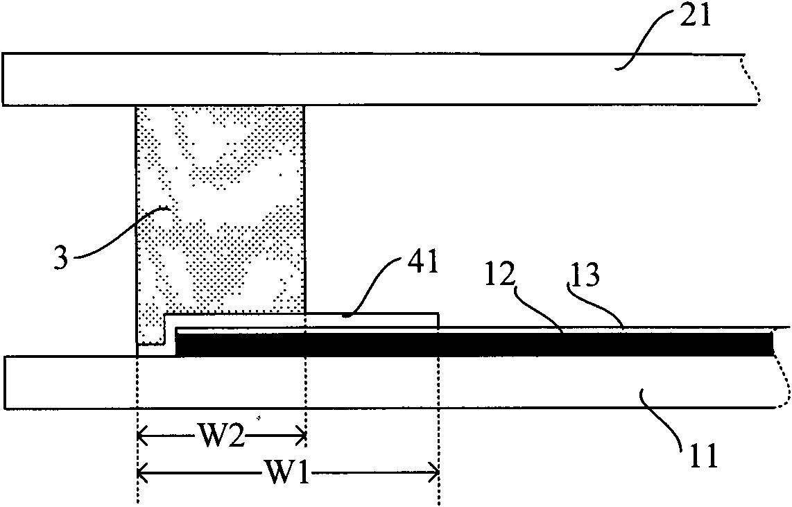
[0027] figure 1 It is a schematic diagram of the structure of the peripheral region of the LCD panel provided by the first embodiment of the present invention. In this embodiment, a light-reflecting layer (hereinafter referred to as the first light-reflecting layer) is formed on a side of the peripheral area of the CF substrate facing the sealant, that is, the first light-reflection layer and the sealant are located on the same side of the CF substrate. like figure 1 As shown, the liquid crystal display panel of this embodiment includes: a CF substrate and an array substrate, and the CF substrate and the array substrate are disposed opposite to each other up and down.
[0028] The array substrate mainly includes: a second transparent substrate 21 and an array structure pattern formed on the second transparent substrate 21 . The array structure pattern is the same as that of the prior art. For example, the array structure pattern (not shown) includes: a gate line pattern, a...
Embodiment 2
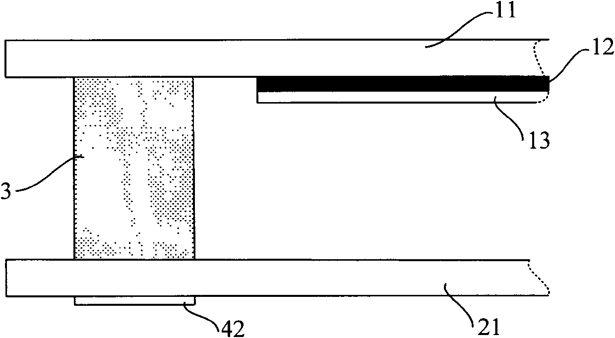
[0041] figure 2 It is a schematic diagram of the structure of the peripheral area of the LCD panel provided by the second embodiment of the present invention. like figure 2 As shown, the difference between the LCD panel of this embodiment and the LCD panel of the first embodiment of the present invention is that the LCD panel of this embodiment is formed with a reflective layer (hereinafter referred to as the first Two reflective layers 42 ), that is, the second reflective layer 42 and the sealant 3 are located on two opposite sides of the array substrate. Specifically, the second reflective layer 42 and the array pattern are respectively formed on two opposite surfaces of the second transparent substrate 21, the second reflective layer 42 is formed on the side of the second transparent substrate 21 close to the backlight source, and at least partially covers the The array substrate is used for coating or aligning the corresponding area of the sealant 3 to reflect the ...
Embodiment 3
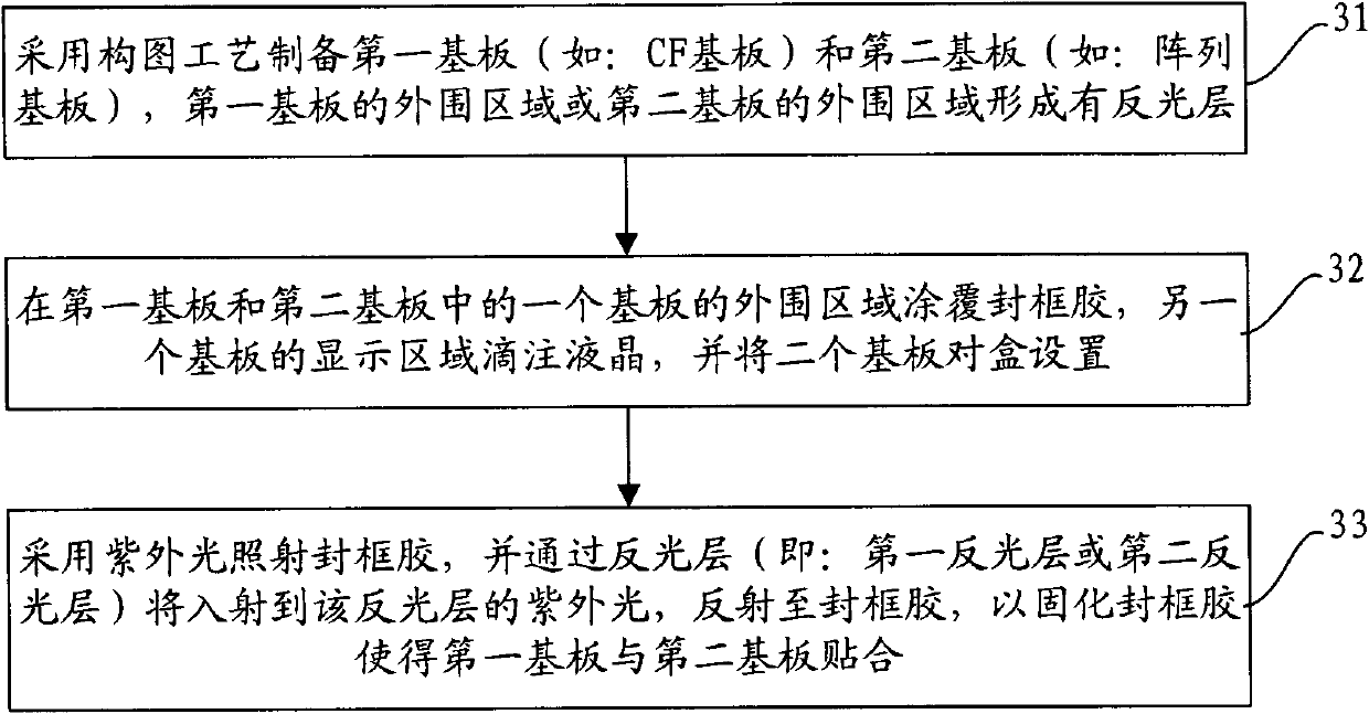
[0055] image 3 It is a flow chart of the manufacturing method of the LCD panel provided by the third embodiment of the present invention. like image 3 As shown, the manufacturing method of the LCD panel of the present embodiment includes:
[0056] Step 31: Prepare the first substrate (such as CF substrate) and the second substrate (such as array substrate) by patterning process, the peripheral area of the first substrate or the peripheral area of the second substrate is formed with a reflective layer.
[0057] For TFT-LCD, the two substrates that make up the LCD panel are: CF substrate and array substrate. It may be advisable to use the CF substrate as the first substrate in this embodiment, and use the array substrate as the second substrate in this embodiment.
[0058] If a reflective layer (that is, the first reflective layer) is formed on the peripheral area of the CF substrate, the first reflective layer is formed on the side of the peripheral area of the CF ...
PUM
| Property | Measurement | Unit |
|---|---|---|
| thickness | aaaaa | aaaaa |
| thickness | aaaaa | aaaaa |
Abstract
Description
Claims
Application Information
 - R&D
- Intellectual Property
- Life Sciences
- Materials
- Tech Scout
- Unparalleled Data Quality
- Higher Quality Content
- 60% Fewer Hallucinations
Browse by: Latest US Patents, China's latest patents, Technical Efficacy Thesaurus, Application Domain, Technology Topic, Popular Technical Reports.
© 2025 PatSnap. All rights reserved.Legal|Privacy policy|Modern Slavery Act Transparency Statement|Sitemap|About US| Contact US: help@patsnap.com