Digital background calibration circuit
A calibration circuit and background technology, applied in the direction of analog/digital conversion calibration/test, analog-to-digital converter, etc., can solve the problems of operational amplifier gain influence, capacitor mismatch, etc., achieve simple algorithm, reduce system power consumption, and reduce chips area effect
- Summary
- Abstract
- Description
- Claims
- Application Information
AI Technical Summary
Problems solved by technology
Method used
Image
Examples
Embodiment Construction
[0015] The digital background calibration circuit of the present invention will be described in detail below in conjunction with the accompanying drawings.
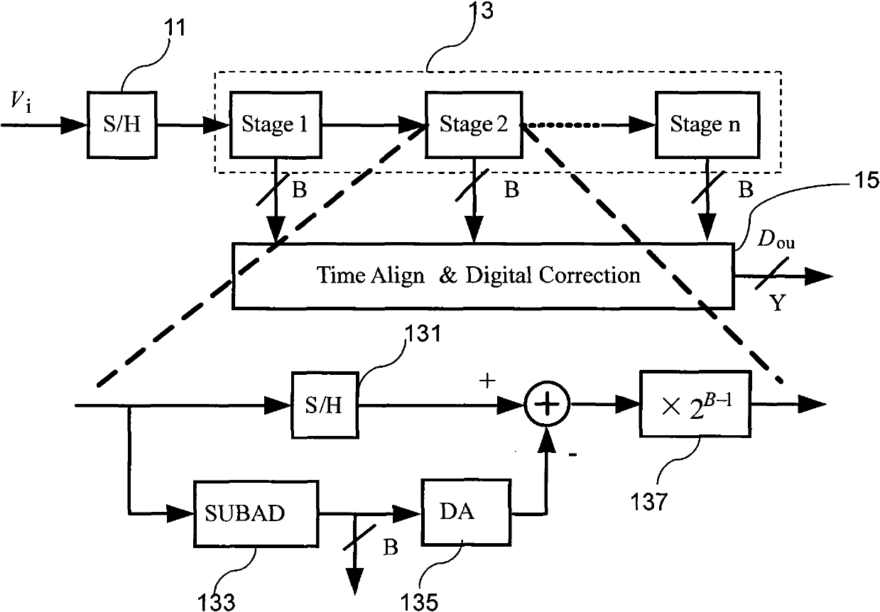
[0016] The basic idea of the pipelined analog-to-digital converter with the traditional structure is to evenly distribute the overall required conversion accuracy to each stage, and the conversion results of each stage are merged into the final conversion result. figure 1 its basic structure. From figure 1 As can be seen in the figure, the pipeline ADC mainly includes a sample-and-hold circuit, n-stage pipeline-level modules, time alignment and correction circuits. Except that the last stage is a fully parallel structure, each stage of the pipeline has the same structure, which consists of an internal sample-and-hold circuit, a low-resolution sub-analog converter, a sub-digital-analog converter, and a residual gain circuit.
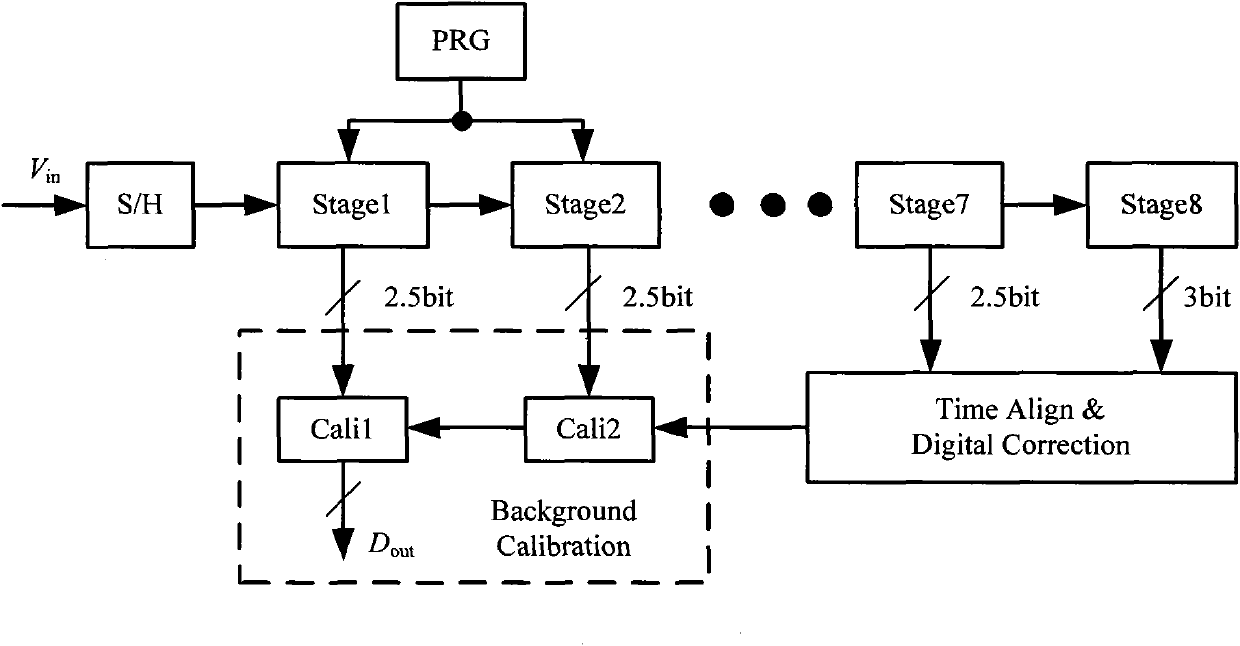
[0017] figure 2 It is the overall structure diagram after adding the calibration circuit. ...
PUM
 Abstract
Description
Claims
Application Information


