Method for preparing wave-absorbing material

A technology of wave-absorbing materials and base materials, applied in the direction of electrical components, magnetic field/electric field shielding, etc., can solve problems such as difficult breakthroughs in the performance of wave-absorbing materials, and achieve the effect of improving wave-absorbing performance and magnetoelectric effect

Inactive Publication Date: 2011-04-27
NO 52 INST OF CHINA NORTH IND GRP CORP
View PDF5 Cites 9 Cited by
  • Summary
  • Abstract
  • Description
  • Claims
  • Application Information

AI Technical Summary

Problems solved by technology

[0003] However, in the study of absorbing materials, the absorption capacity of traditional absorbing materials is mainly concentrated in the frequency band above 5GHz, and

Method used


Image

  • Method for preparing wave-absorbing material
  • Method for preparing wave-absorbing material
  • Method for preparing wave-absorbing material

Examples


Embodiment 1

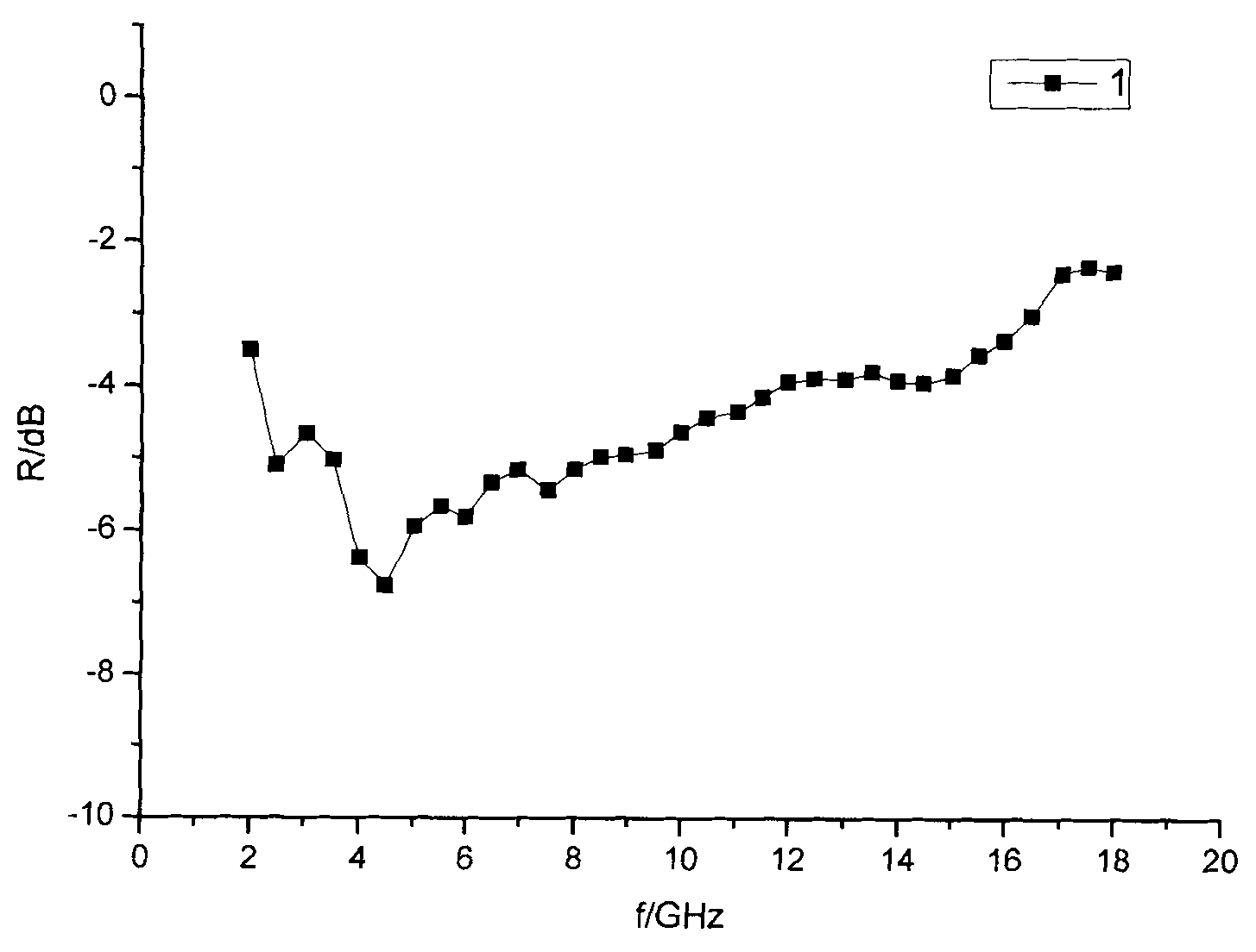
[0021] The material composition of this example is Fe 72 Cu 1 Nb 3 Si 15 B 9 , the iron-based nanocrystalline material base material is prepared by a single-roll chilling method, and the material is subjected to nanocrystallization treatment under the protection of high-purity nitrogen gas to obtain a nanocrystalline material with a nanocrystalline phase structure. The iron-based nanocrystalline material is mechanically crushed by a high-speed cutting method to prepare a nanocrystalline material powder, and the powder is sieved to obtain a graded powder of 45 μm to 60 μm. The powder is reprocessed with jet mill equipment, the gas working pressure is 0.5MPa, the treatment time is 1h, and then its absorbing performance is measured. Such as figure 1 As shown, it can be seen that the reflectance R=-3.5dB at 2GHz, and the maximum emissivity appears at the frequency point of 4.5GHz, which is -6.7dB. In the frequency range of 2GHz to 18GHz, the bandwidth of reflectivity greater ...

Embodiment 2

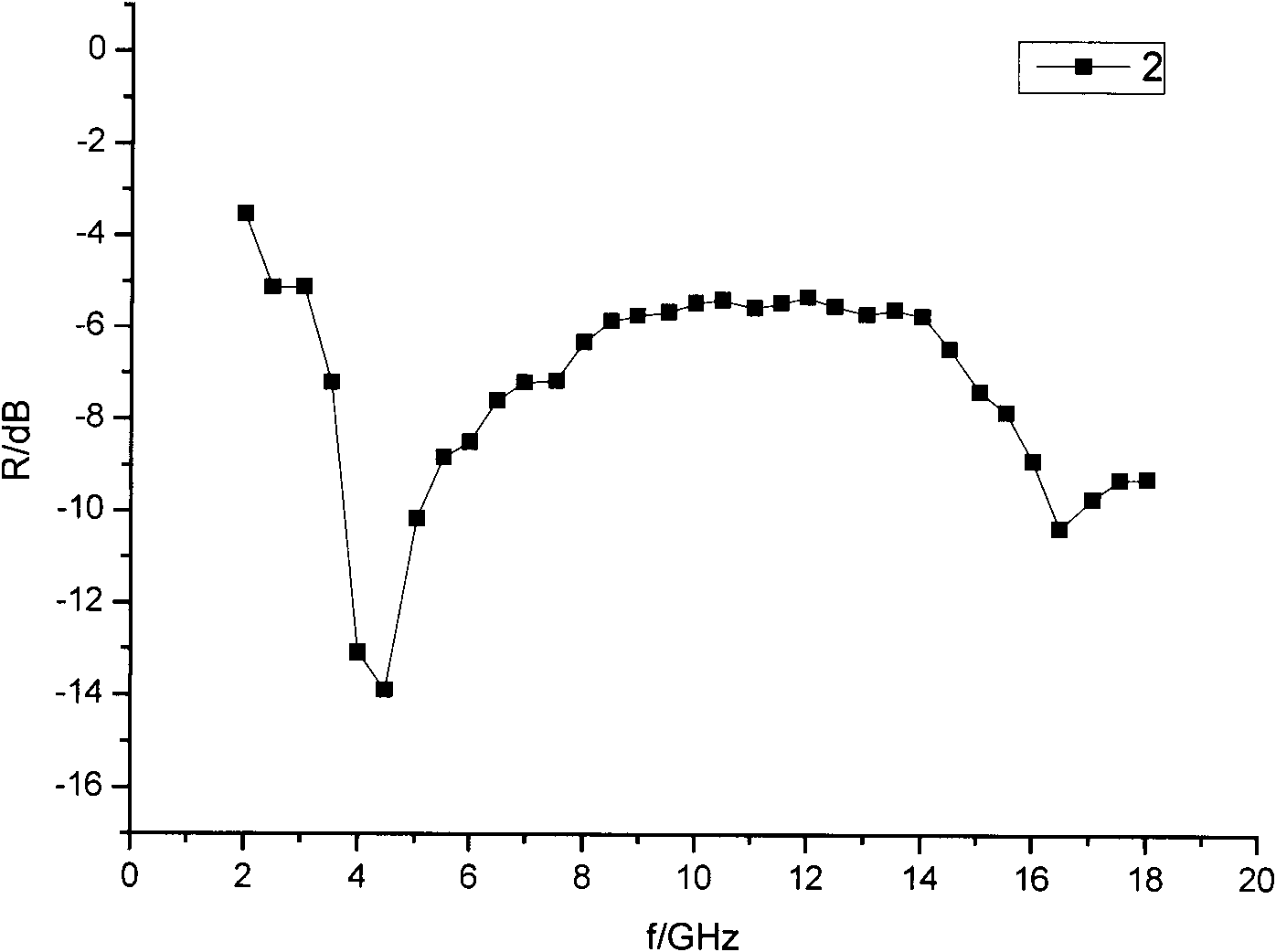
[0023] The material composition of this example is Fe 72.5 Cu 1 Nb 2 V 2 Si 13.5 B 9 , the iron-based nanocrystalline material base material is prepared by a single-roll chilling method, and the material is subjected to nanocrystallization treatment under the protection of high-purity nitrogen gas to obtain a nanocrystalline material with a nanocrystalline phase structure. The iron-based nanocrystalline material is mechanically crushed by a high-speed cutting method to prepare a nanocrystalline material powder, and the powder is sieved to obtain a graded powder of 45 μm to 60 μm. The powder is reprocessed with jet mill equipment, the gas working pressure is 1.0MPa, the treatment time is 3h, and then its absorbing performance is measured, such as figure 2 As shown, it can be seen that the reflectivity R=-3.5dB at 2GHz, and the maximum reflectivity appears at the frequency point of 4.5GHz, which is -13.9dB. In the frequency range of 2GHz to 18GHz, the bandwidth with reflec...

Embodiment 3

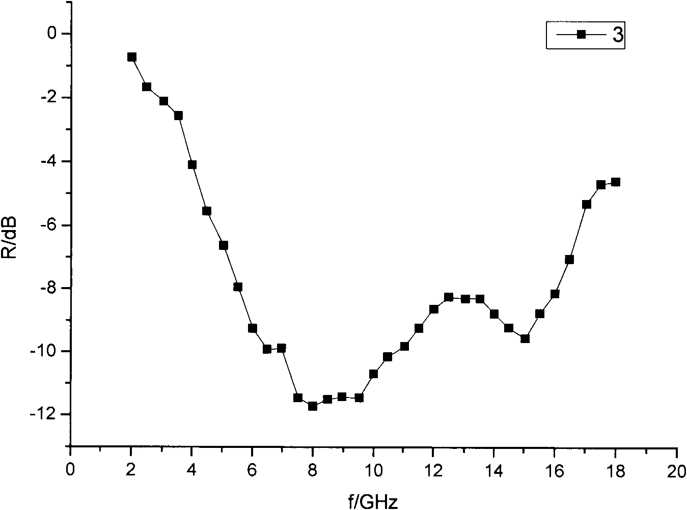
[0025] The material composition of this example is Fe 73.5 Cu 1 Nd 3 Si 13.5 B 9 , the iron-based nanocrystalline material base material is prepared by a single-roll chilling method, and the material is subjected to nanocrystallization treatment under the protection of high-purity nitrogen gas to obtain a nanocrystalline material with a nanocrystalline phase structure. The iron-based nanocrystalline material is mechanically crushed by a high-speed cutting method to prepare a nanocrystalline material powder, and the powder is sieved to obtain a graded powder with a level of 30 μm to 45 μm. The powder is reprocessed with jet mill equipment, the gas working pressure is 1.0MPa, the treatment time is 3h, and then its absorbing performance is measured, such as image 3 As shown, it can be seen that the reflectivity R=-0.75dB at 2GHz, and the maximum reflectivity appears at the frequency point of 8GHz, which is -11.7dB. In the frequency range of 2GHz to 18GHz, the bandwidth with ...


PUM

PropertyMeasurementUnit
Reflectivityaaaaaaaaaa
Emissivityaaaaaaaaaa
Reflectivityaaaaaaaaaa

Abstract

The invention discloses a method for preparing a wave-absorbing material, which is characterized by comprising the following steps of: 1, performing nanocrystallization treatment on a base material of an iron-based nanocrystalline material prepared by a single-roll quenching method under the protection of nitrogen to obtain an iron-based nanocrystalline material with a nano crystalline phase structure; 2, performing mechanical crushing on the iron-based nanocrystalline material through high-speed cutting to obtain powder; and 3, reprocessing the powder by using a jet mill for 0.5 to 4 hours under the gas pressure of 0.5-2.0MPa. Compared with the prior art, the method has the advantages that: the powder is refined through high-speed collision of the jet mill, and the micromorphology of the powder material is changed by a method for modifying the micromorphology of the nanocrystalline magnetic powder, so that the magneto-electrical properties of the powder are changed and the aim of improving the magnetoelectric effect and wave-absorbing property of the material is fulfilled.

Description

technical field [0001] The invention relates to a method for preparing an absorbing material, specifically, an iron-based nanocrystalline material is used as a parent material. Background technique [0002] Electromagnetic wave pollution has become an important problem in today's world. With the development and application of 3G mobile phones, high-frequency computer chips, and the popularization of microwave ovens, electromagnetic pollution has penetrated into all aspects of life, and has had a serious impact on environmental safety. In addition, the information leakage and interference of electromagnetic waves also cause great harm to the security of important information for military and civilian use, and the research and development of electromagnetic wave absorbing materials has always been an important topic. Public documents on this aspect in the prior art can refer to CN101445716A, CN100518480C, CN101567224A, etc. [0003] However, in the study of absorbing material...

Claims


Application Information

Patent Timeline
IPC IPC(8): C22C38/00C22C1/04H05K9/00
Inventor 钱坤明纪松吴敏丁昂张延松李明利
Owner NO 52 INST OF CHINA NORTH IND GRP CORP
Why Eureka
Try Eureka