Method for realizing static and dynamic random access memory (SDRAM) refresh by using field programmable gate array (FPGA)

A refresh cycle and refresh time technology, applied in information storage, static memory, digital memory information, etc., can solve problems such as huge power consumption, increased circuit design, and increased power consumption of system circuits.

Active Publication Date: 2013-06-12
曙光网络科技有限公司
View PDF2 Cites 0 Cited by
  • Summary
  • Abstract
  • Description
  • Claims
  • Application Information

AI Technical Summary

Problems solved by technology

[0004] In Patent No. 00102790.5 "Dynamic Random Access Memory that Can Selectively Perform Self-refresh Operation of Memory Banks", a method of reducing the power consumption of DRAM is mentioned. This method only targets those memory banks that store data when refreshing. Refresh, unlike the traditional refresh is for all memory banks, so that the system power consumption can be reduced by targeted selective refresh, but this method needs to increase the circuit design when it is applied to a large-capacity, multi-memory system, and additional Increases the circuit power consumption of the system, and the patent is only for the power reduction of the self-refresh operation
[0005] The method for reducing memory bank refresh power consumption mentioned in Patent No. 200510071912.9 "Self-refresh control device and method based on memory bank in semiconductor memory device", this method also selectively refreshes during self-refresh operation, can Effectively reduce the self-refresh current and power consumption. This method does not mention how to reduce the huge power consumption caused by the self-refresh operation, and in the field of large-capacity and multi-memory, additional circuits are required to maintain it, which also brings additional power overhead

Method used


Image

  • Method for realizing static and dynamic random access memory (SDRAM) refresh by using field programmable gate array (FPGA)

Examples


Embodiment Construction

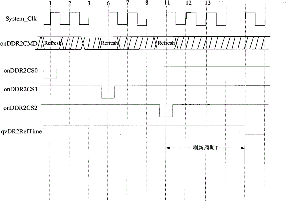
[0016] as attached figure 1 shown. If there are three chip select CSs in the current memory controller that need to be refreshed, when the specified refresh time arrives, as shown in the first clock cycle in the figure, the FPGA sends a refresh command to select the first chip select CS0. The refresh cycle is not over. After CS0 starts to refresh for 5 cycles, issue the second refresh command to select the second chip selection CS1. Also after CS1 strobe refreshes for 5 cycles, issue the third refresh command and select the second chip selection at the same time. The three chip selects CS2, because the memory models are the same, on the premise that the refresh cycle of CS2 is satisfied, the refresh cycles of CS0 and CS1 must also be satisfied. Under normal circumstances, after starting the CS0 refresh, if the refresh period is T, you must wait for the end of the refresh period T before starting the refresh of CS1, and so on, the time required to refresh the three chip select...


PUM


Abstract

The invention provides a novel method for realizing static and dynamic random access memory (SDRAM) refresh by using field programmable gate array (FPGA). In a memory controller, N chip selections (CS) are required to be refreshed; at a preset refresh time, a refresh command is sent to gate a first chip selection CS0; before the refresh period of the CS0 ends and after the CS0 starts M periods, arefresh command is started to gate a second chip selection CS1; and in the same way, all memories are refreshed. When the technical scheme is adopted, the refresh current and refresh power consumption of SDRAM particles are reduced effectively. The method has obvious power consumption reducing effect particularly when used in a large-capacity and multi-memory system, so the method can effectivelyreduce the machine power consumption in the system.

Description

technical field [0001] The invention relates to the design of a memory controller, in particular to a method for reducing SDRAM refresh power consumption realized by FPGA. Background technique [0002] There are two types of semiconductor memory devices, dynamic random access memory (DRAM) and static random access memory (SRAM). The SRAM internally stores data in the form of a bistable circuit, which can save the internally stored data without refreshing the circuit. The storage unit of DRAM is composed of transistors and capacitors. The data is stored in the capacitor. Since the capacitor will leak electricity, the data stored in the capacitor will be destroyed as time goes by. Therefore, the data stored in the capacitor needs to be periodically repeatedly charged. DRAM that can work synchronously with the CPU clock is called SDRAM. [0003] The refresh of SDRAM is divided into two modes: auto refresh (auto refresh, AR) and self refresh (self refresh, SR). Regardless of...

Claims


Application Information

Patent Timeline
Patent Type & Authority Patents(China)
IPC IPC(8): G11C11/406
Inventor 李静李楠宁白宗元张磊张英文纪奎
Owner 曙光网络科技有限公司
Why Eureka
Try Eureka