Method for epitaxial growth of molecular beam of low-density InAs quantum dots
A technology of molecular beam epitaxy and growth method, applied in the field of molecular beam epitaxy growth, can solve the problems of limited extraction efficiency, low growth, difficulty in density single-photon source long-wavelength quantum dots, etc., and achieve the effect of improving luminous efficiency and increasing collection efficiency.
- Summary
- Abstract
- Description
- Claims
- Application Information
AI Technical Summary
Problems solved by technology
Method used
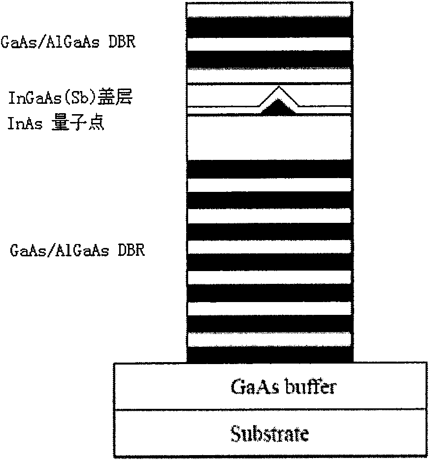
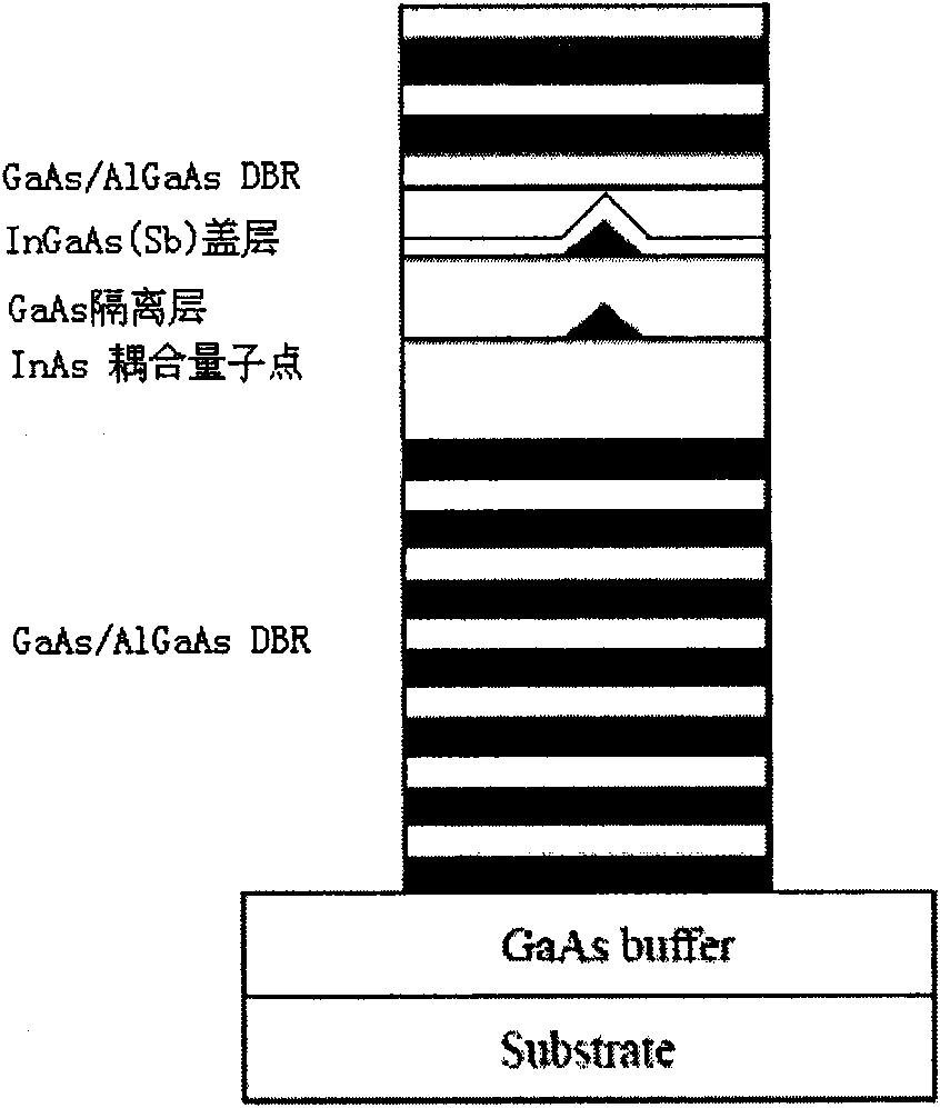
Image

Examples
Embodiment
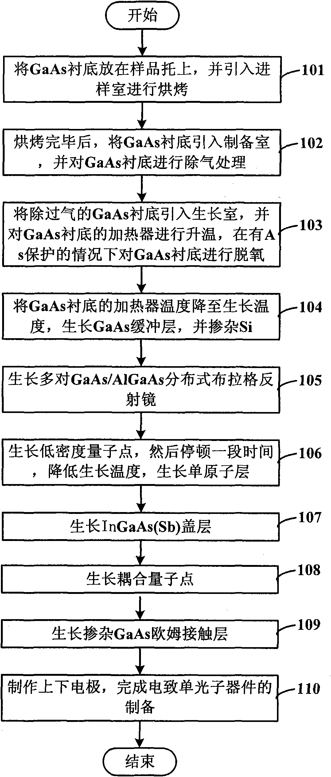
[0071] In this embodiment, Veeco GEN II molecular beam epitaxy equipment is used for growth.
[0072] The GaAs (100) substrate is placed on the sample holder, and introduced into the sample chamber for baking at a temperature of 180-250 degrees Celsius.
[0073] The baked substrate is introduced into the preparation chamber and degassed at 400-450 degrees Celsius, and the atmospheric pressure in the buffer chamber is reduced to 10 -8 When the Torr is below, the degassing is complete.
[0074] The degassed substrate is introduced into the growth chamber, and the temperature of the substrate heater is raised, and the sample is deoxidized under the protection of As. Deoxidation temperature range: 580 to 620 degrees Celsius, deoxidation time 5 minutes.
[0075] During the deoxidation process, the atomic reconstruction on the surface of the substrate was observed with the help of a reflection high-energy electron diffractometer (RHEED) to determine whether it was deoxidized.
[...
PUM
| Property | Measurement | Unit |
|---|---|---|
| Thickness | aaaaa | aaaaa |
| Thickness | aaaaa | aaaaa |
| Doping concentration | aaaaa | aaaaa |
Abstract
Description
Claims
Application Information
 - R&D
- Intellectual Property
- Life Sciences
- Materials
- Tech Scout
- Unparalleled Data Quality
- Higher Quality Content
- 60% Fewer Hallucinations
Browse by: Latest US Patents, China's latest patents, Technical Efficacy Thesaurus, Application Domain, Technology Topic, Popular Technical Reports.
© 2025 PatSnap. All rights reserved.Legal|Privacy policy|Modern Slavery Act Transparency Statement|Sitemap|About US| Contact US: help@patsnap.com