Method for manufacturing metal gate

A manufacturing method and metal gate technology, which are applied in semiconductor/solid-state device manufacturing, electrical components, semiconductor devices, etc., can solve problems such as thinning, unevenness of silicon substrate 1, and inability of lithography machine to focus accurately.

Inactive Publication Date: 2011-05-04
SEMICON MFG INT (SHANGHAI) CORP
View PDF0 Cites 11 Cited by
  • Summary
  • Abstract
  • Description
  • Claims
  • Application Information

AI Technical Summary

Problems solved by technology

After cleaning, the silicon substrate 1 becomes thinner and uneven, which leads to the pro

Method used


Image

  • Method for manufacturing metal gate
  • Method for manufacturing metal gate
  • Method for manufacturing metal gate

Examples


Example Embodiment

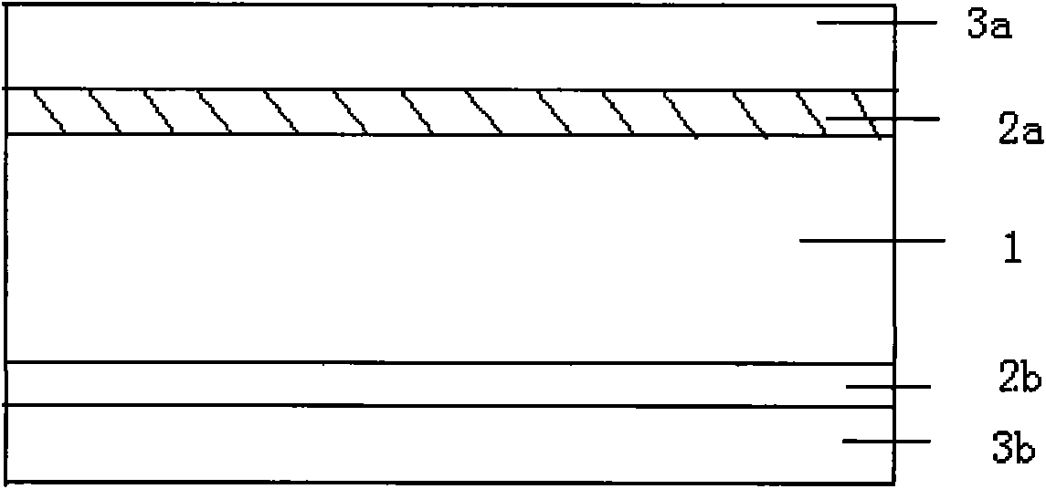
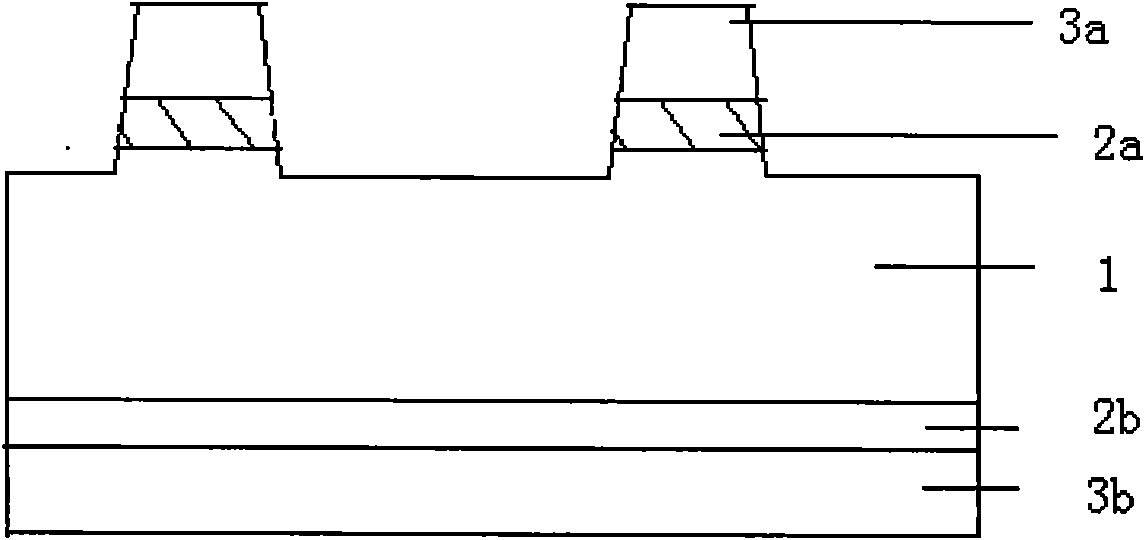
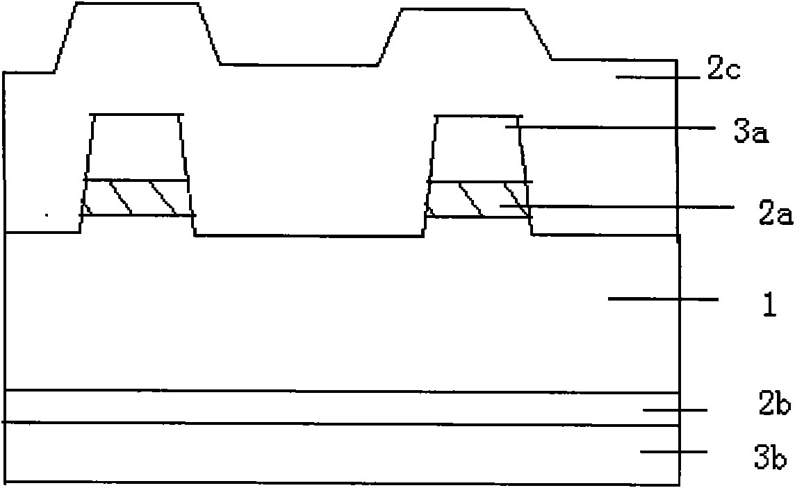
[0018] In the embodiment of the present invention, dry etching and wet etching are used together to etch the protective layer on the wafer to prevent the protective layer under the silicon substrate of the wafer from being etched simultaneously when only wet etching is used. Since the metal atom contamination will directly contaminate the silicon substrate and diffuse into the silicon substrate when etching the metal gate, the contaminated silicon substrate needs to be cleaned before entering the next process, otherwise it will affect the wafer Quality, but the cleaned substrate makes the back surface uneven, which not only makes the wafer unable to focus accurately in subsequent processes such as lithography.

[0019] In order to make the above objects, features and advantages of the present invention more comprehensible, specific implementations of the present invention will be described in detail below in conjunction with the accompanying drawings.

[0020] figure 2 For m...


PUM

PropertyMeasurementUnit
Thicknessaaaaaaaaaa
Thicknessaaaaaaaaaa

Abstract

The invention relates to a method for manufacturing a metal gate, comprising the following steps: firstly providing a wafer with a silicon base, respectively forming a first oxide layer and a second oxide layer on the front surface and the back surface of the silicon base, and respectively forming a first protective layer and a second protective layer on the first oxide layer and the second oxide layer; etching the first protective layer, the first oxide layer and the silicon base; depositing third oxide layers on the first protective layer and an exposed silicon base, and flattening the third oxide layer until the first protective layer is exposed; removing part of the first protective layer by using dry etching; removing the residual first protective layer and part of second protective layer by using wet etching; forming a well region, and removing the first oxide layer by precleaning to form a gate oxide layer; and forming the metal gate. Metal atoms which are exposed out of the side of a grid do not spread to the silicon base, so that the silicon substrate with a certain thickness at the back of the wafer is in no need of removing after the metal gate is etched, thus avoiding the problems that the loss of silicon atoms are resulted from the uneven back surface of the wafer to influence the sequent exposure, and the like.

Description

technical field [0001] The invention relates to the field of semiconductors, in particular to a metal gate manufacturing method. Background technique [0002] In the field of integrated circuit manufacturing, especially in the 32nm process, the method of using high-K materials and metal gates will be widely adopted. There are two basic etching processes in semiconductor manufacturing to etch metal gates: dry etching and wet etching. Dry etching is to expose the surface of the wafer to the plasma generated in the gaseous state. The plasma passes through the window opened by the photoresist and reacts with the wafer physically or chemically, thereby removing the exposed surface material. Dry etching is the most important method for etching devices with submicron dimensions. In wet etching, however, liquid chemicals chemically remove material from the wafer surface. Wet etching can be used to etch certain layers on the wafer or to remove residues after dry etching. [0003]...

Claims


Application Information

Patent Timeline
IPC IPC(8): H01L21/28H01L21/311H01L21/318
Inventor 周地宝任红茹
Owner SEMICON MFG INT (SHANGHAI) CORP
Why Eureka
Try Eureka