Method for positioning low impedance tiny flaws in comb metal wire structure

A metal wire, low-impedance technology, applied in the field of failure analysis and positioning, can solve the problem of not finding defects, achieve fast positioning, high efficiency, and save manpower

Inactive Publication Date: 2011-05-11
SHANGHAI HUA HONG NEC ELECTRONICS
View PDF0 Cites 24 Cited by
  • Summary
  • Abstract
  • Description
  • Claims
  • Application Information

AI Technical Summary

Problems solved by technology

[0008] The beneficial effect of the present invention is that it provides a method for accurately locating fine defects in comb-shaped aluminum wires, which has fast positioning speed and high efficiency, and on the one hand, it

Method used


Image

  • Method for positioning low impedance tiny flaws in comb metal wire structure
  • Method for positioning low impedance tiny flaws in comb metal wire structure
  • Method for positioning low impedance tiny flaws in comb metal wire structure

Examples


Embodiment Construction

[0016] Such as Figure 6 The illustrated invention comprises the following steps:

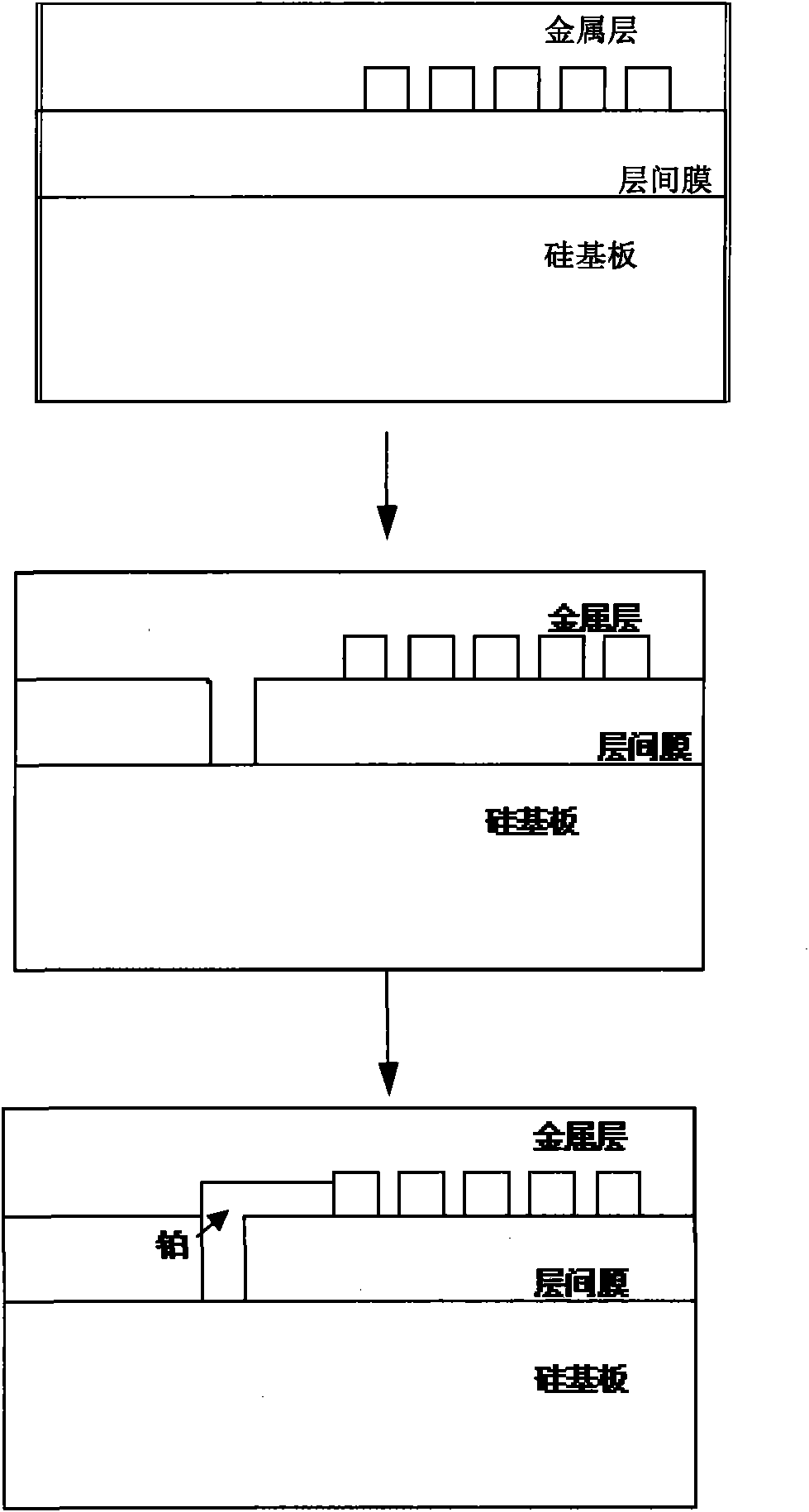
[0017] Step 1. If figure 1 As shown, the focused particle beam electron microscope FIB is used to perforate the silicon substrate (the silicon substrate is usually the ground terminal), and the platinum-plated metal layer of the focused particle beam electron microscope FIB is used to connect one end of the comb line to the substrate to achieve grounding.

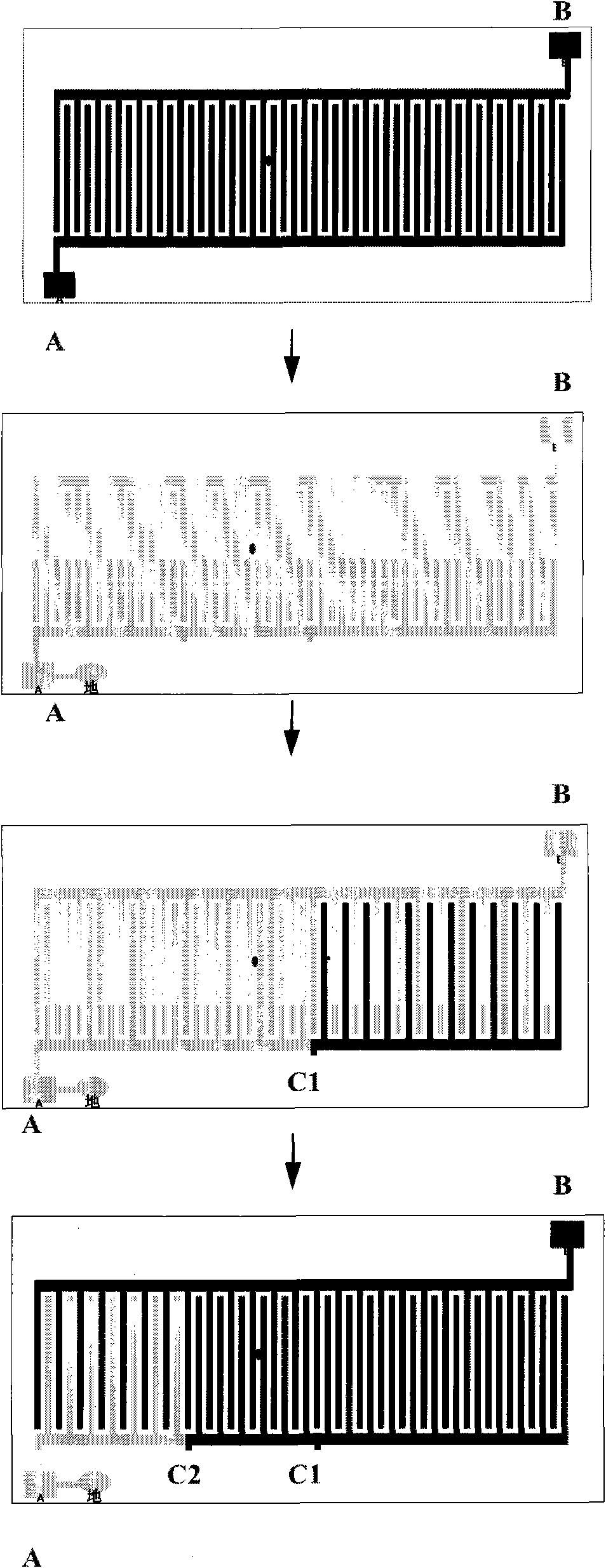
[0018] Step 2. If figure 2 As shown, the comb line is divided into n times, and each time is divided into a voltage contrast VC inspection, and each time the voltage contrast VC can locate the defect within half of the original area, n times After equal division, the defect will be located within the area range of 1 / 2 to the nth power.

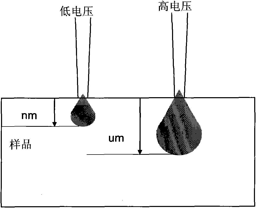
[0019] Step 3. If image 3 As shown, in the small area positioned, the defects buried by the insulating film can be observed by scanning the scanning electron microscope SEM with a high accelerating vol...


PUM


Abstract

The invention discloses a method for positioning low impedance tiny flaws in a comb metal wire structure, comprising the following steps: step one, punching a hole to an earthed terminal by a focused ion beam electron microscope (EMS), and realizing one end of a comb meal wire to be earthed by adopting a focused ion beam electron microscope metallic coating; step two, dividing the comb metal wire into n equal parts, wherein primary voltage contrast detection is performed at each time of dividing, the flaws can be positioned within the halved original area by each voltage contrast, and the flaws can be positioned within the area range of one [n(th) powder]th after evenly dividing for n times, and n is a positive integer; and step three, in the positioned tiny area, adopting an electron microscope for high accelerating voltage scanning to obverse the flaws buried by an insulating film. The method in the invention has high positioning speed and high efficiency, can solve the problem that flaws of some metal growth etching related technologies in semiconductor production lines can not be found out, and can greatly save manpower and use time of the electron microscope for scanning.

Description

technical field [0001] The invention relates to a failure analysis and positioning technology for semiconductor chips, in particular to a positioning method for low-impedance tiny defects in a comb-shaped metal wire structure. Background technique [0002] At present, the methods for locating tiny defects in comb-shaped metal wire structures can be roughly divided into the following categories: [0003] 1. Observation with an optical microscope. The disadvantage is that due to the limitation of resolution greater than 1 micron, defects smaller than 1 micron cannot be observed. [0004] 2. Use a scanning electron microscope to magnify and observe, and the resolution can reach several nanometers. Its defect is: but because generally at least thousands of comb-shaped metal wires are interlaced together, and the area is often more than 100 microns by 100 microns, it takes a long time to find defects smaller than 1 micron. [0005] 3. Photo-induced impedance change technology,...

Claims


Application Information

Patent Timeline
IPC IPC(8): G01N23/22G01Q80/00
Inventor 赖华平
Owner SHANGHAI HUA HONG NEC ELECTRONICS
Why Eureka
Try Eureka