Method for improving filling capacity of wafer channel

A technology of filling ability and trench, which is applied in the direction of electrical components, semiconductor/solid-state device manufacturing, circuits, etc., to achieve the effect of avoiding hole defects and orderly arrangement

Inactive Publication Date: 2013-01-30
SEMICON MFG INT (SHANGHAI) CORP
View PDF4 Cites 0 Cited by
  • Summary
  • Abstract
  • Description
  • Claims
  • Application Information

AI Technical Summary

Problems solved by technology

[0004] However, for the high-density plasma chemical vapor deposition technology, only in the STI process with an aspect ratio of less than 6.0 or the PMD process with an aspect ratio of less than 2.7, there will be no hole defects when filling the trench; for As far as the high aspect ratio process technology is concerned, only in the STI process with an aspect ratio of less than 7.0 or the PMD process with an aspect ratio of less than 3.0 will there be no hole defects when filling the trench
Therefore, the trench filling technology in the prior art can only guarantee that there will be no hole defects when the aspect ratio is less than 7.0

Method used


Image

  • Method for improving filling capacity of wafer channel
  • Method for improving filling capacity of wafer channel

Examples


Embodiment Construction

[0036] In order to better understand the technical content of the present invention, specific embodiments are given and described as follows in conjunction with the accompanying drawings.

[0037] The invention proposes a method for improving the filling capacity of the wafer trench, which can effectively meet the technical requirements of higher aspect ratio in the new technology.

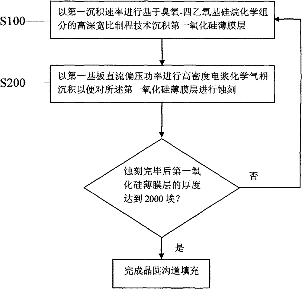
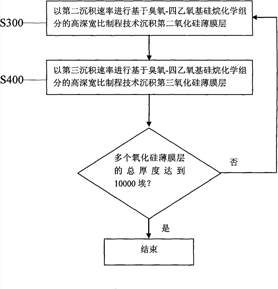
[0038] Please refer to figure 1 , figure 1 Shown is a flow chart of a method for improving the trench filling capability of a wafer according to a preferred embodiment of the present invention. The present invention proposes a method for improving the filling capability of the wafer trench, wherein a trench is formed on the wafer, and the method comprises the following steps:

[0039] Step S100: Depositing a first silicon oxide thin film layer in the trench with a high aspect ratio process technology based on the chemical composition of ozone-tetraethoxysilane at a first deposition rate;

[004...


PUM


Abstract

The invention provides a method for improving the filling capacity of a wafer channel. A channel is formed on a wafer. The method comprises the following steps: step 100, depositing a first silicon oxide thin layer in the channel at a first rate of deposition based on a high aspect ratio processing technology of ozone-tetraethoxysilane chemical components; step 200, carrying out high-density plasma chemical vapor deposition by DC bias power of a first substrate so as to facilitate etching the first silicon oxide thin layer; and repeating step 100 and step 200 in sequence until the thickness of the first silicon oxide thin layer reaches 2000 angstrom after the etching is over, thus finishing the filling of the wafer channel. The method for improving the filling capacity of the wafer channel can be used to effectively meet the high aspect ratio processing requirements in the new process.

Description

technical field [0001] The invention relates to the manufacturing field of semiconductor devices, and in particular to a method for improving the filling capability of wafer trenches. Background technique [0002] In the field of semiconductor manufacturing, high density plasma chemical vapor deposition (High Density Plasma Chemical Vapor Deposition, HDP-CVD) with good filling ability, better film deposition characteristics and higher filling efficiency is usually used to deposit oxide in shallow trenches. Silicon thin film to form a shallow trench isolation structure (Shallow Trench Isolation, STI), a pre-metal dielectric layer (Pre-Metal Dielectric, PMD) or an inter-metal dielectric layer (Inter-Metal Dielectric, IMD) . However, with the continuous reduction of the minimum feature size of semiconductor devices, the size of STI is also reduced accordingly. When the minimum feature size of semiconductor devices is reduced to 65 nanometers and below, the HDP-CVD process has ...

Claims


Application Information

Patent Timeline
Patent Type & Authority Patents(China)
IPC IPC(8): H01L21/762H01L21/316
Inventor 李景伦
Owner SEMICON MFG INT (SHANGHAI) CORP
Why Eureka
Try Eureka