Multi-component gradient-doping GaN UV (Ultraviolet) light cathode material structure and manufacture method thereof

A technology of gradient doping and cathode material, which is applied in the manufacture of light-emitting cathodes, photo-emission cathodes, main electrodes of discharge tubes, etc., can solve the problems of small escape ratio of photoexcited electrons, improve the overall quantum efficiency and increase the escape depth. , the effect of high UV sensitivity

Inactive Publication Date: 2011-05-18
NANJING UNIV OF SCI & TECH
View PDF2 Cites 19 Cited by
  • Summary
  • Abstract
  • Description
  • Claims
  • Application Information

AI Technical Summary

Problems solved by technology

However, the escape ratio of photoexcited electrons in the deeper part of the emissive layer is s

Method used


Image

  • Multi-component gradient-doping GaN UV (Ultraviolet) light cathode material structure and manufacture method thereof
  • Multi-component gradient-doping GaN UV (Ultraviolet) light cathode material structure and manufacture method thereof
  • Multi-component gradient-doping GaN UV (Ultraviolet) light cathode material structure and manufacture method thereof

Examples


Embodiment 1

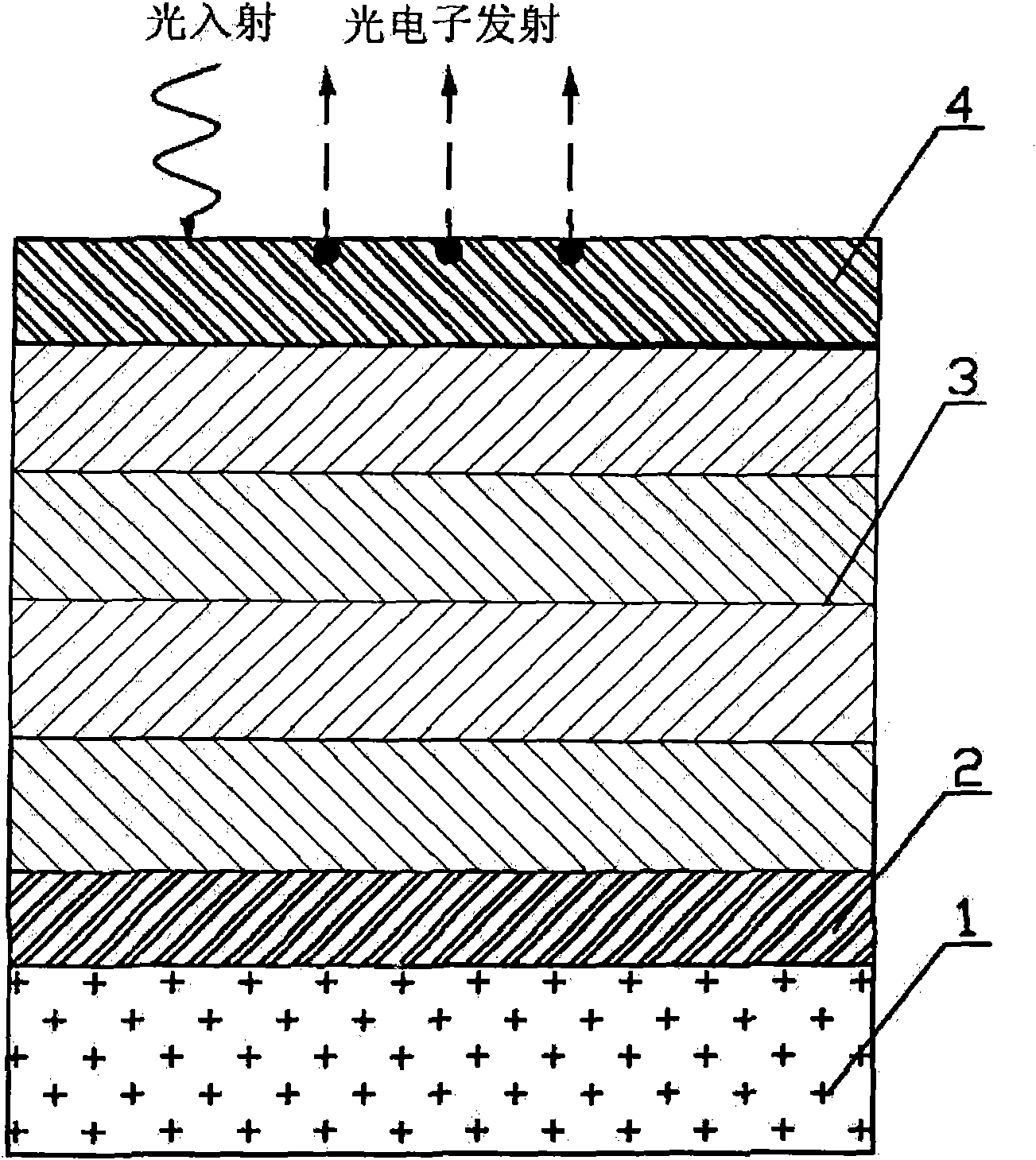
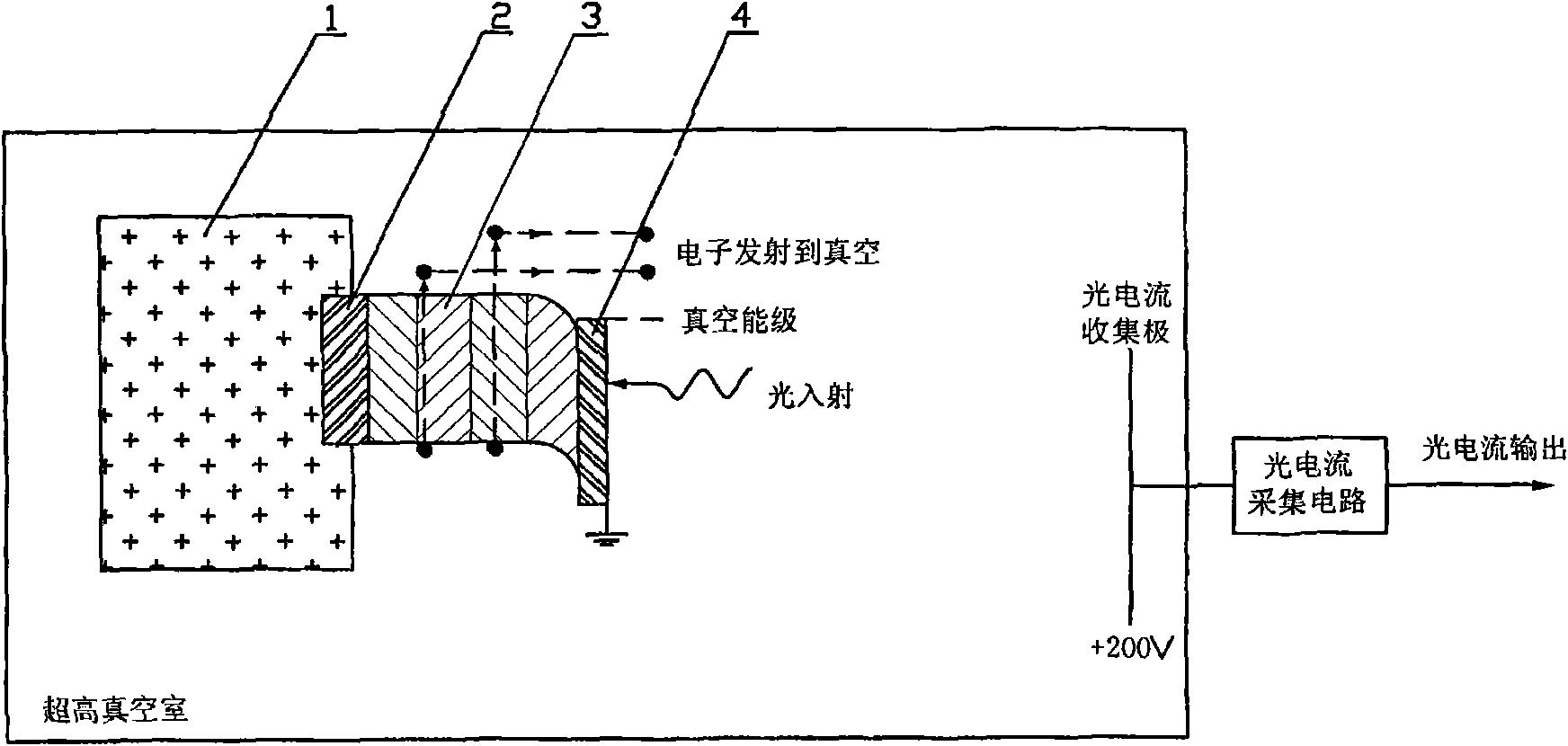
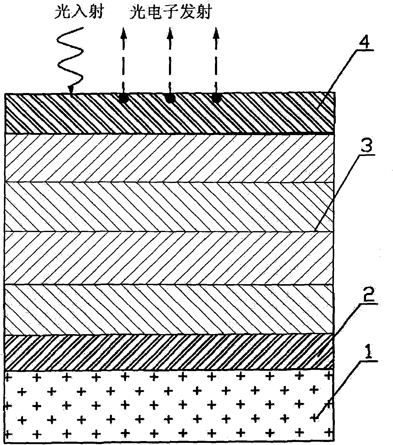
[0024] Embodiment 1: as figure 1 As shown, a reflective GaN ultraviolet photocathode material structure, the material structure consists of substrate 1 (such as sapphire), unintentionally doped AlN buffer layer 2, p-type Ga x Al 1-x N multi-component mixed crystal photoemissive layer 3 and Cs or Cs / O active layer 4; wherein, unintentionally doped AlN buffer layer 2 is epitaxially grown on the substrate layer 1 with a thickness of 50nm; p-type Ga x Al 1-x The N multi-component mixed crystal photoelectric emission layer 3 is epitaxially grown on the aforementioned AlN buffer layer 2 with a thickness of 120 nm and a doping concentration of 1×10 18 , 4×10 17 , 2×10 17 and 6×10¹⁶ , gradually decreases from the body to the body surface, the proportion control parameter x in the mixed crystal takes the AlN buffer layer as the growth starting point, and gradually changes from 0 to 1; the Cs active layer 4 is adsorbed on the p-type Ga x Al 1-x On the front surface of the N multi-...

Embodiment 2

[0025] Embodiment 2: Different from Embodiment 1, the thickness of the AlN buffer layer is 100nm; p-type Ga x Al 1-x The N multi-component mixed crystal photoelectric emission layer 3 is epitaxially grown on the aforementioned AlN buffer layer 2 with a thickness of 120 nm and a doping concentration of 1×10 18 , 4×10 17 , 2×10 17 and 6×10 16 , gradually decreases from the body to the body surface, the proportion control parameter x in the mixed crystal takes the AlN buffer layer as the growth starting point, and gradually changes from 0 to 1; the Cs active layer 4 is adsorbed on the p-type Ga x Al 1-x On the front surface of the N multi-component mixed crystal photoelectric emission layer 3, the thickness is one monoatomic layer.

Embodiment 3

[0026] Embodiment 3: Different from Embodiment 1, the thickness of the AlN buffer layer is 100nm; p-type Ga x Al 1-x The N multi-component mixed crystal photoelectric emission layer 3 is epitaxially grown on the aforementioned AlN buffer layer 2 with a thickness of 150 nm and a doping concentration of 1×10 18 , 4×10 17 , 2×10 17 and 6×10 16 , gradually decreases from the body to the body surface, the proportion control parameter x in the mixed crystal takes the AlN buffer layer as the growth starting point, and gradually changes from 0 to 1; the Cs active layer 4 is adsorbed on the p-type Ga x Al 1-x On the front surface of the N multi-component mixed crystal photoelectric emission layer 3, the thickness is one monoatomic layer.


PUM

PropertyMeasurementUnit
Thicknessaaaaaaaaaa
Thicknessaaaaaaaaaa
Thicknessaaaaaaaaaa

Abstract

The invention provides a reflection-type GaN UV (Ultraviolet) light cathode material structure and a manufacture method thereof. The structure comprises a substrate, an involuntarily doping AlN buffer layer, a p-type GaxAI1-xN multi-component mix-crystal photoelectric emission layer and a Cs or Cs /O active layer, wherein the involuntarily doping AlN buffer layer grows on the substrate; the p-type GaxAI1-xN multi-component mix-crystal photoelectric emission layer epitaxially grows on the AlN buffer layer; and the Cs or Cs /O active layer is absorbed on the front surface of the p-type GaxAI1-xN multi-component mix-crystal photoelectric emission layer and has the thickness of an nm order of magnitude. By adopting the multi-component and gradient-doping photoelectric emission layer, the structure increases the escape depth of photonexcited electrons in the emission layer and improves the possibility for emitting the electrons in the emission layer into vacuum so as to improve the whole quantum efficiency of the GaN UV light cathode and acquire higher UV sensibility.

Description

technical field [0001] The invention belongs to the technical field of ultraviolet detection materials, and in particular relates to a reflective ultraviolet photocathode material structure and a manufacturing method based on the combination of semiconductor material epitaxy technology, semiconductor material doping technology and ultra-high vacuum surface activation technology. Background technique [0002] In recent years, with the improvement of GaN material preparation technology, p-type doping technology and the development of ultra-high vacuum technology, GaN UV photocathode is becoming a new type of high-performance UV photocathode. The surface of this cathode has a negative electron affinity (Negative Electron Affinity, NEA), that is, the surface vacuum energy level of the cathode is lower than the bottom energy level of the conduction band in the body. Through emission into vacuum, there is no need for excess kinetic energy to overcome the potential barrier on the s...

Claims


Application Information

Patent Timeline
IPC IPC(8): H01L31/0224H01J1/34H01L31/18H01J9/12
CPCY02P70/50
Inventor 常本康李飙徐源杜玉杰王晓晖杜晓晴
Owner NANJING UNIV OF SCI & TECH
Why Eureka
Try Eureka