Semiconductor chip assembly with post/base heat spreader and substrate

A technology for semiconductors and heat sinks, applied in the field of semiconductor chip assemblies, can solve the problems of limited routing capability, too large volume, and unsuitable for low-cost mass production operations.

Inactive Publication Date: 2011-05-18
BRIDGE SEMICON
View PDF11 Cites 10 Cited by
  • Summary
  • Abstract
  • Description
  • Claims
  • Application Information

AI Technical Summary

Problems solved by technology

If the substrate is a single-layer circuit system, the routing capability is limited, but if the substrate is a multi-layer circuit system, its excessively thick dielectric layer will reduce the heat dissipation effect
In addition, the previous technology also has problems such as insufficient heat sink performance, too large volume, or difficult thermal connection to the next layer of assembly.
The manufacturing process of the previous technology is not suitable for low-cost mass production

Method used


Image

  • Semiconductor chip assembly with post/base heat spreader and substrate
  • Semiconductor chip assembly with post/base heat spreader and substrate
  • Semiconductor chip assembly with post/base heat spreader and substrate

Examples


Embodiment Construction

[0076] In order to further explain the technical means and effects of the present invention to achieve the intended purpose of the invention, in conjunction with the accompanying drawings and preferred embodiments, the following is a description of the semiconductor chip set with the heat sink of the boss / substrate and the substrate according to the present invention. The detailed description of its specific implementation, structure, features and effects is as follows.

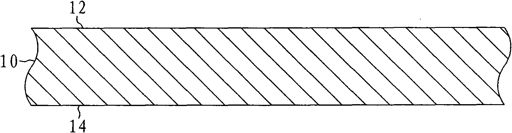
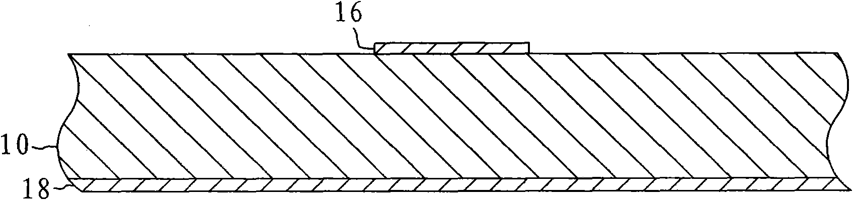
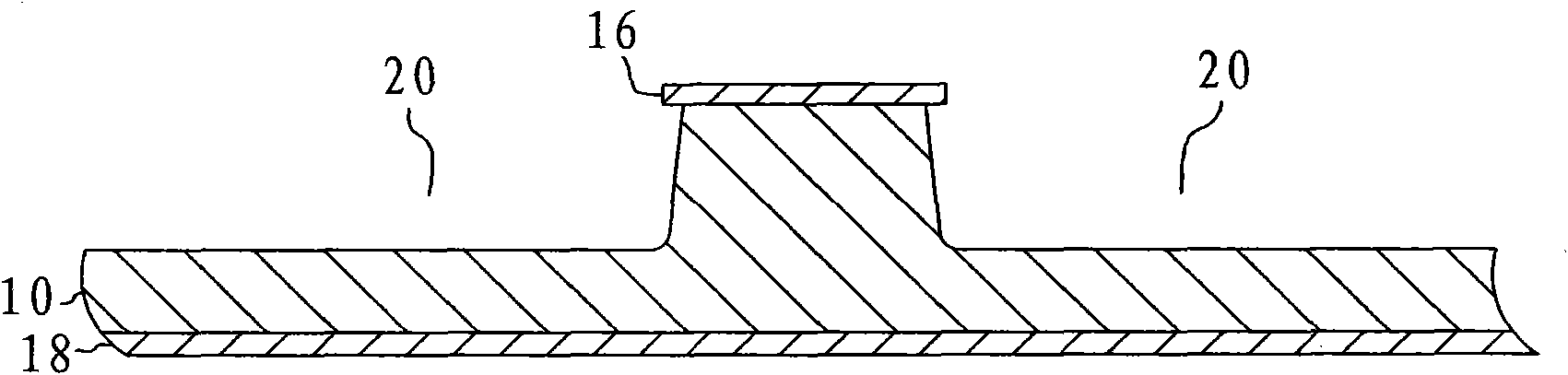
[0077] Figure 1 to Figure 4 It is a cross-sectional view illustrating a method of manufacturing a protrusion and a base in an embodiment of the present invention. Figure 5 and Image 6 Respectively Figure 4 Top view and bottom view of.

[0078] figure 1 It is a cross-sectional view of the metal plate 10, and the metal plate 10 includes main surfaces 12 and 14 opposite to each other. The illustrated metal plate 10 is a copper plate with a thickness of 500 microns. Copper has the advantages of high thermal condu...


PUM


Abstract

The invention relates to a semiconductor chip assembly with a post/base heat spreader and a substrate. The semiconductor chip assembly at least includes a semiconductor device, the heat spreader, the substrate and an adhesive. The semiconductor device is electrically connected to the substrate and thermally connected to the heat spreader. The heat spreader at least includes a post and a base. Thepost extends upwardly from the base into an opening in the adhesive and an aperture in the substrate, and the base extends laterally from the post. The adhesive extends between the post and the substrate and between the base and the substrate.The assembly provides signal routing between a pad and a terminal.

Description

Technical field [0001] The invention relates to a semiconductor chip assembly, in particular to a semiconductor chip assembly composed of a semiconductor element, a substrate, an adhesive layer and a heat sink, and a manufacturing method thereof. Background technique [0002] Semiconductor components such as packaged and unpackaged semiconductor chips can provide high-voltage, high-frequency and high-efficiency applications; these applications require high power consumption to perform specific functions, but the higher the power, the production of semiconductor components. The more heat. In addition, as the packaging density is increased and the size is reduced, the surface area available for heat dissipation is reduced, resulting in increased heat generation. [0003] Semiconductor components are prone to problems such as performance degradation and shortened service life under high temperature operation, and may even fail immediately. High heat not only affects chip performance...

Claims


Application Information

Patent Timeline
Patent Type & Authority Applications(China)
IPC IPC(8): H01L33/48H01L33/64H01L33/62H01L25/075
CPCH01L2224/48091H01L2224/49171H01L2924/181
Inventor 林文强王家忠
Owner BRIDGE SEMICON
Why Eureka
Try Eureka