

Normally off gallium nitride field effect transistors (fet)
A gallium nitride and gallium nitride layer technology, applied in the field of normally off gallium nitride field effect transistors, can solve device reliability problems, reduce transconductance, low inversion mobility and other problems
- Summary
- Abstract
- Description
- Claims
- Application Information
AI Technical Summary
Problems solved by technology
Method used
Image

Examples
Embodiment Construction
[0019] The following combination Figure 2 to Figure 7 , to describe preferred embodiments of the present invention in detail.
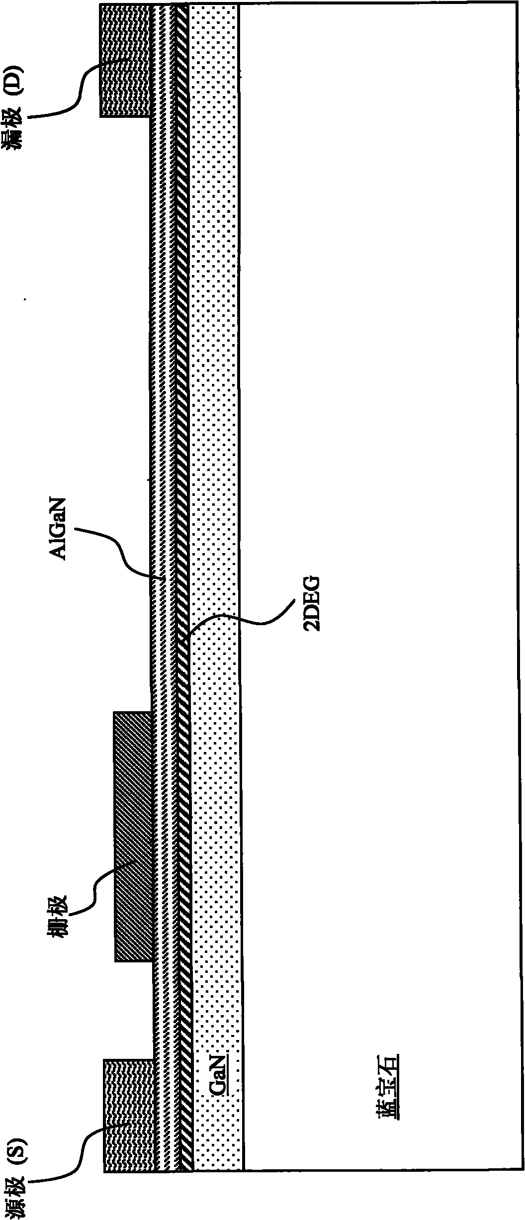
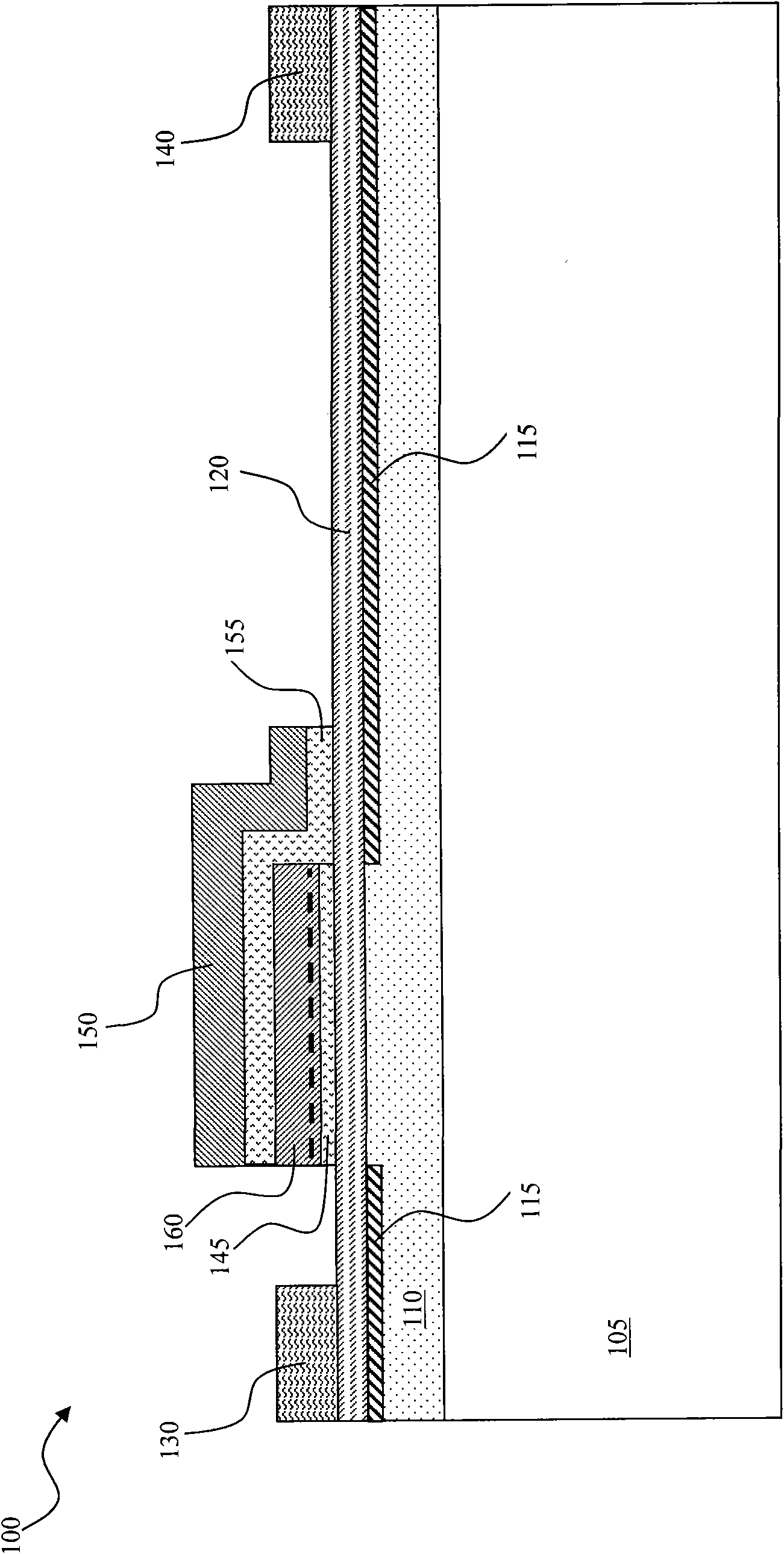
[0020] Please refer to figure 2 , a cross-sectional view of a heterojunction field effect transistor (HFET) semiconductor power device 100 according to the present invention. The HFET semiconductor power device 100 includes an AlGaN layer 120 epitaxially grown on a Gallium Nitride (GaN) layer 110, thereby forming an AlGaN / GaN heterojunction with a two-dimensional electron gas (2DEG) 115 at the interface . The source electrode 130 and the drain electrode 140 are disposed on two opposite sides of the gate electrode 150 to control current flow through the 2DEG layer 115 . The gate electrode 150 is insulated from the N-doped AlGaN layer 120 by a thicker gate oxide layer 155 . To configure the HFET power device as a normally-off device, the floating gate 160 is formed under at least a portion of the gate oxide layer 155 . Floating gate 160 is insula...
PUM
 Abstract
Description
Claims
Application Information