Method for designing testability of chip

A design method and testing technology, applied in the field of DFT insertion, simulation and static timing analysis, logic synthesis, can solve the test method without a complete system, DFT tools, logic synthesis tools, circuit simulation and other tools can not achieve connection, design Program complexity, etc.

Active Publication Date: 2011-06-01
西安翔腾微电子科技有限公司
View PDF1 Cites 26 Cited by
  • Summary
  • Abstract
  • Description
  • Claims
  • Application Information

AI Technical Summary

Problems solved by technology

[0004] In order to solve the technical problems that there is no complete system of testing methods for different test objects in the existing chip design process, DFT tools, logic synthesis tools, circuit simulation and other tools cannot be con

Method used


Image

  • Method for designing testability of chip
  • Method for designing testability of chip
  • Method for designing testability of chip

Examples


Embodiment

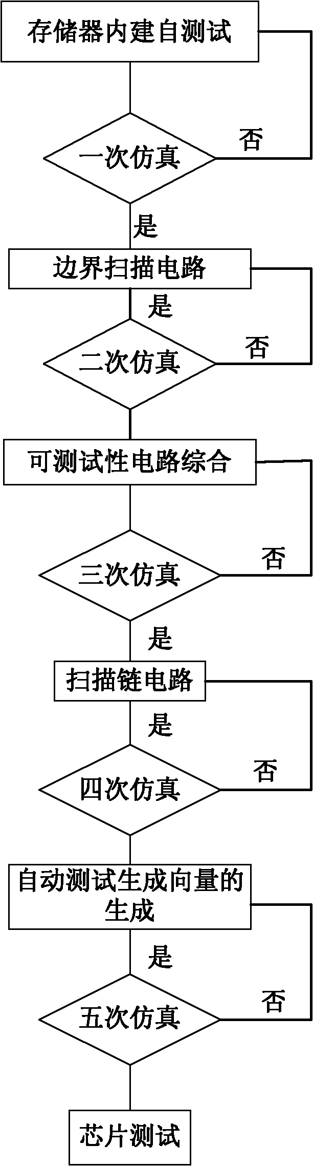
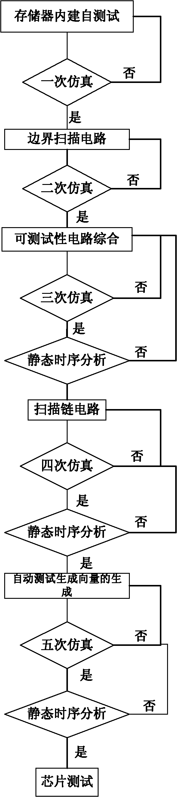
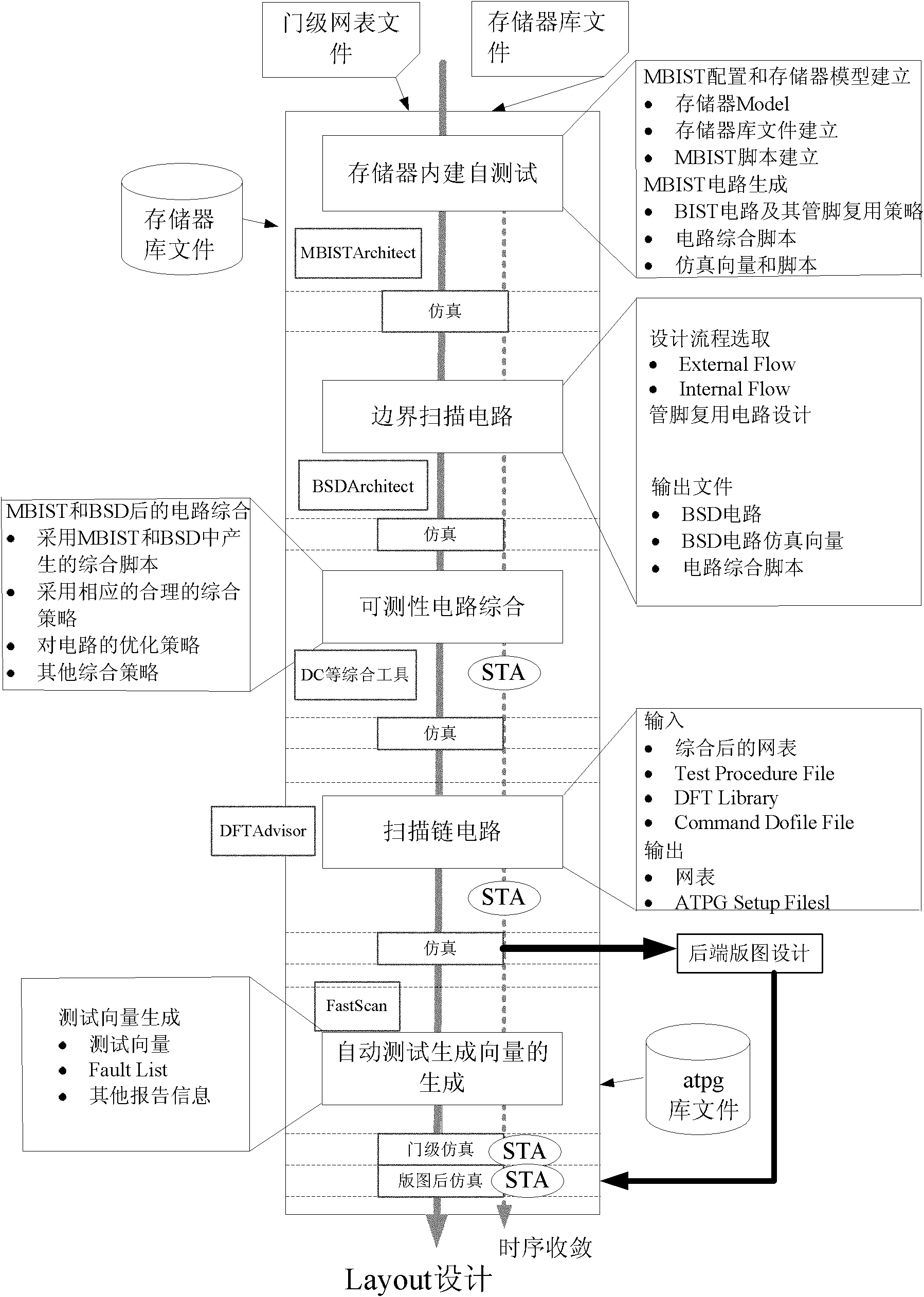
[0122] This process is mainly based on Mentor's DFT tools (MBISTArchitect, BSDArchitect, FastScan, DFTAdvisor), Synopsys' DC synthesis tool, Mentor's simulation tool ModelSim and other tools to complete a typical SoC-based DFT design and test vector production and simulation.

[0123] (1) Synthesize the RTL code into a gate-level netlist file based on the process library using synthesis tools from companies such as SynopSys.

[0124] (2) Write the storage library files required by Mentor's MBISTArchitect. After these two steps are completed, the preparation for DFT design is completed.

[0125] (3) Use the MBISTArchitect tool memory built-in self-test circuit of Mentor Company to insert the MBIST circuit. The specific implementation script is:

[0126] mbistarchitect. / netlist / mydesign_fix_timing.v-verilog\

[0127] -top mydesign_top \

[0128] -lverilog . / libs / *.v\

[0129] -logfile mbist.log-replace\

[0130] ...


PUM


Abstract

The invention relates to a method for designing testability of a chip, which comprises the steps: (1) insertion of a built-in self test circuit of a memory; (2) insertion of a boundary scan circuit; (3) integration of a testability circuit; (4) insertion of a scan chain circuit; and (5) generation of automatic test generated vectors. In order to solve the technical problems that in the traditional chip design process, a set of complete and systematical method in test methods aiming at different test objects is not available, tools such as a DFT (diagnostic function test) tool, a logic synthesis tool, a circuit simulation tool and the like are not joined and the design program is complicated, the invention provides the process guarantee for automation of the DFT design and complete and systematical correctness of the DFT design.

Description

technical field [0001] The invention relates to a chip design method, in particular to a method for DFT insertion, logic synthesis, simulation and static timing analysis. Background technique [0002] DFT (Design For Testability) is an attempt to increase the controllability and observability of signals in the circuit, so as to test whether there are physical defects in the chip in a timely and economical manner, so that users can get good chips. Why do DFT? Because in the chip design process, that is, what is handed over from the register transfer level RTL to GDSII is only a layout, and finally the chip needs to be manufactured in the factory, that is, the manufacturer makes the chip according to the data you provide GDSII. Defects may occur during this process. This defect may be physically present, or it may be caused by a legacy problem in the design. On the other hand, defects may also occur during the packaging process. In order to ensure that our chips do not have ...

Claims


Application Information

Patent Timeline
IPC IPC(8): G06F17/50
Inventor 田泽郭蒙蔡叶芳李攀杨海波
Owner 西安翔腾微电子科技有限公司
Why Eureka
Try Eureka