Power inductor and manufacturing method thereof

A technology of power inductors and manufacturing methods, which is applied in the field of SMD power inductors and its manufacturing, can solve problems such as large size, and achieve the effects of improving product Q value, reducing RDC, improving DC bias characteristics and current resistance characteristics

Active Publication Date: 2011-06-01
SHENZHEN MICROGATE TECH
View PDF7 Cites 4 Cited by
  • Summary
  • Abstract
  • Description
  • Claims
  • Application Information

AI Technical Summary

Problems solved by technology

The wire-wound inductors in the traditional process are increasingly unable to meet people's needs due to their large size.

Method used


Image

  • Power inductor and manufacturing method thereof
  • Power inductor and manufacturing method thereof
  • Power inductor and manufacturing method thereof

Examples


Embodiment 1

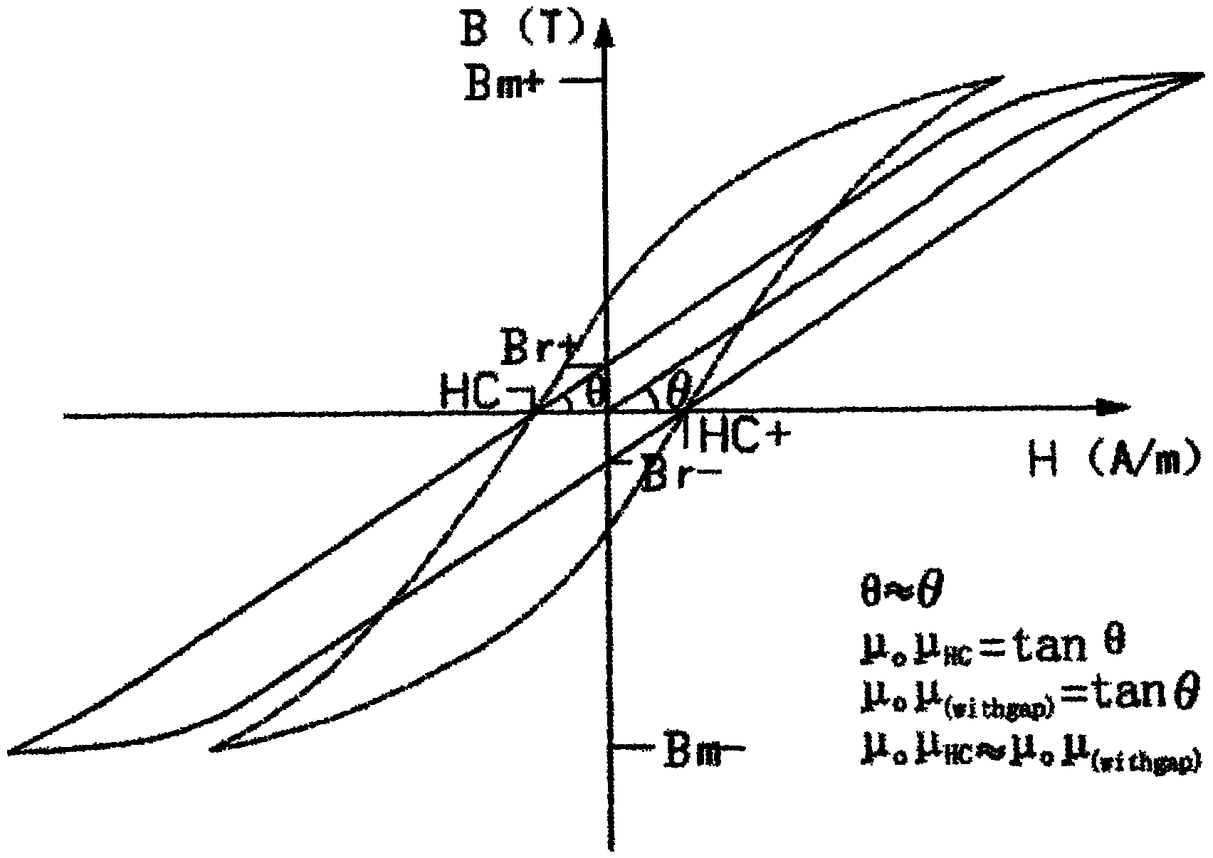
[0064] Embodiment 1: In this embodiment, the main component of ferrite includes Fe with a molar ratio of 45%. 2 o 3 , CuO with a molar ratio of 12%, NiO with a molar ratio of 13%, and ZnO with a molar ratio of 30%; the first added component is BI 2 o 3 The molar ratio to the main component is 0.001:100; the molar ratio of each component in the second added component to the main component is 0.003:100. After testing, the ferrite material in this embodiment can have a saturation magnetic flux density Bs of 470 mT or above under an applied magnetic field of 4000 A / m.

Embodiment 2

[0065] Embodiment 2: In this embodiment, the main component of ferrite includes Fe with a molar ratio of 45%. 2 o 3 , CuO with a molar ratio of 10%, NiO with a molar ratio of 25%, and ZnO with a molar ratio of 30%; the first added component is BI 2 o 3 The molar ratio to the main component is 0.002:100; the molar ratio of each component in the second added component to the main component is 0.005:100. After testing, the ferrite material in this embodiment can have a saturation magnetic flux density Bs of 470 mT or above under an applied magnetic field of 4000 A / m.

Embodiment 3

[0066] Embodiment 3: In this embodiment, the main component of ferrite includes Fe with a molar ratio of 50%. 2 o 3 , CuO with a molar ratio of 17%, NiO with a molar ratio of 18%, and ZnO with a molar ratio of 20%; the first added component is BI 2 o 3 The molar ratio to the main component is 0.002:100; the molar ratio of each component in the second added component to the main component is 0.005:100. After testing, the ferrite material in this embodiment can have a saturation magnetic flux density Bs of 470 mT or above under an applied magnetic field of 4000 A / m.


PUM

PropertyMeasurementUnit
thicknessaaaaaaaaaa
thicknessaaaaaaaaaa
saturation flux densityaaaaaaaaaa

Abstract

The invention discloses a chip type power inductor and a manufacturing method thereof. The inductor comprises a substrate, an inductance coil, a terminal stud and a dielectric layer, wherein the inductance coil is arranged in the substrate in a stacking manner, and both ends of the inductance coil are respectively connected with the terminal stud; and the dielectric layer is arranged in the substrate and separates the power inductor into an upper layer and a lower layer. After the inductor is formed by adopting a casting process and a lining electrode printing process, a finished product is manufactured through low temperature cofiring. Through the special air gap action of the dielectric layer, the characteristics of the stacking inductor are improved, and the DC bias characteristic and the flow resistance characteristic of the stacking power inductor are increased. Compared with a wound power inductor, the stacking power inductor is easier to reduce element size and thickness. The chip type power inductor is applicable to the development of new electronic elements, fills up the national blankness on such components, and has innovation in the aspects of materials, design, processes, measurement and the like. The product has advanced design, a self-developed process route is adopted, and the performance of the product can reach the international advanced level.

Description

technical field [0001] The invention discloses an inductor and a manufacturing method thereof, in particular to a patch type power inductor and a manufacturing method thereof. Background technique [0002] As the functions of electronic mobile terminals continue to increase, their required operating voltages also become diversified. For many battery-powered products such as mobile phones, digital cameras, and PDAs, their LCD backlight drivers, power amplifier modules, and IC power circuits all require different output voltages. Thus, a DC-to-DC converter is required to convert the voltage of the battery power supply into different multiple voltages to supply power to the above functional blocks. Therefore, in order to reduce power consumption and extend battery life, high-efficiency voltage converters are widely used, and the key factor affecting the efficiency of the converter is the power inductor. At the same time, electronic mobile terminals are becoming smaller and th...

Claims


Application Information

Patent Timeline
Patent Type & Authority Applications(China)
IPC IPC(8): H01F17/00H01F37/00H01F41/00
Inventor 张海恩张美蓉张亚平陈鑫
Owner SHENZHEN MICROGATE TECH
Why Eureka
Try Eureka