MOS transistor resistor, filter, and integrated circuit

A technology of MOS transistors and resistors, which is applied in the direction of transistors, circuits, electric solid-state devices, etc., can solve the problems such as difficult to form filters, and achieve the effect of reducing the change of resistance value and good temperature characteristics

Inactive Publication Date: 2011-06-08
PANASONIC CORP
View PDF6 Cites 3 Cited by
  • Summary
  • Abstract
  • Description
  • Claims
  • Application Information

AI Technical Summary

Problems solved by technology

Therefore, it is difficult to construct a filter

Method used


Image

  • MOS transistor resistor, filter, and integrated circuit
  • MOS transistor resistor, filter, and integrated circuit
  • MOS transistor resistor, filter, and integrated circuit

Examples


no. 1 approach

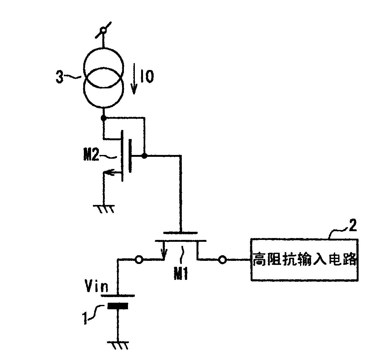
[0086] figure 1 It is a circuit diagram showing the MOS transistor resistor in Embodiment 1. This MOS transistor resistor is composed of MOS transistors M1, M2, and an input voltage source 1 (voltage Vin). The source of the MOS transistor M1 is grounded through the input voltage source 1, and the drain is connected to the high-impedance input (high input impedance) circuit 2 of the subsequent stage circuit. The voltage generated by the MOS transistor M2 and the current source 3 (current I0 ) is applied to the gate of the MOS transistor M1 .

[0087] The operation of the MOS transistor resistor configured as above will be described. In the case of this MOS transistor resistor, the resistance value is also represented by (Expression 4). In addition, in the following description, the same symbols are used to describe the same elements as those used in the description of the conventional art, and the numbers corresponding to the symbols of the MOS transistors are added for des...

no. 2 approach

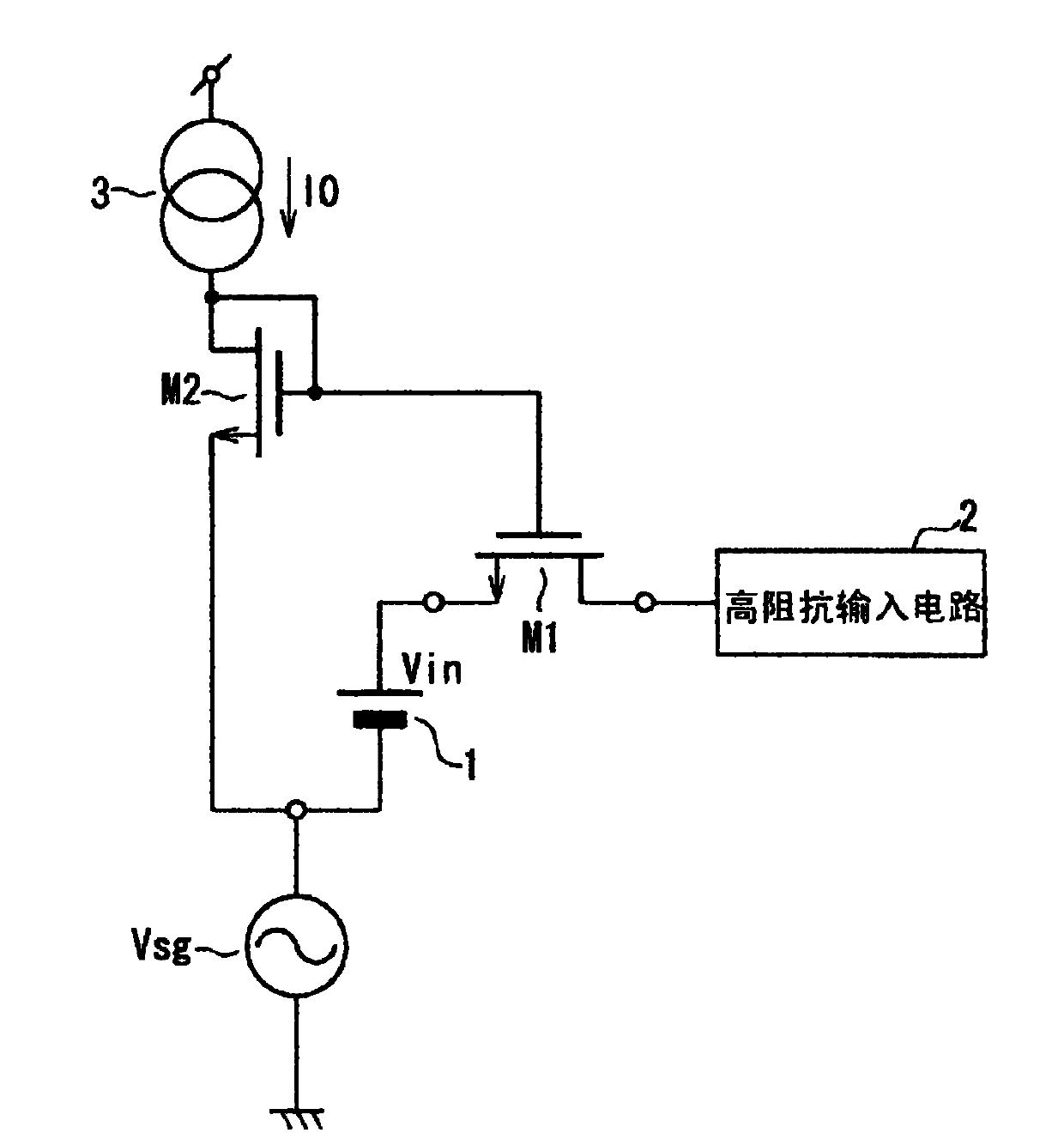
[0122] Figure 10 It is a circuit diagram showing a MOS transistor resistor in Embodiment 2 of the present invention. This MOS transistor resistor differs from figure 1 The structure of the MOS transistor resistor in Embodiment 1 is shown. That is, the voltage Vg of the gate voltage source 6 is applied to the gate of the MOS transistor M1.

[0123] exist Figure 10 In the structure, if the voltage Vg is set to be the same as figure 1 If the value of the gate-source voltage VGS2 of the MOS transistor M2 is the same, the same effect as that of the MOS transistor resistor of Embodiment 1 can be obtained. In other words, if the voltage Vg is set to the gate-source voltage VGS2 represented by (mathematical formula 16), that is, the voltage obtained by adding twice the input voltage to the threshold voltage VTH, the temperature of the resistance value Ron can be eliminated. characteristic.

[0124] As described above, the MOS transistor resistor of this embodiment includes: ...


PUM


Abstract

Disclosed is a MOS transistor resistor that is equipped with a first MOS transistor (M1), which is used as a resistor, an input voltage source (1), which is connected, and applies an input voltage (Vin), to the source of the first MOS transistor, and a gate voltage source (6), which is connected, and applies a gate voltage (Vg), to the gate of the first MOS transistor. The gate voltage (Vg) and input voltage (Vin) are set in a range to cause the first MOS transistor to operate with the gate-source voltage and the source-drain voltage in the first MOS transistor in the unsaturated zone, and are set so that the temperature characteristics at the resistance value of the first MOS transistor become constant. Fluctuations in resistance value, which are caused by changes in leakage current due to manufacturing variances, are decreased and excellent temperature characteristics are obtained.

Description

technical field [0001] The present invention relates to a resistor using a MOS transistor, and particularly to a MOS transistor resistor suitable for use in an electronic device that performs sound signal processing such as a microphone or that performs signal processing including a sensor, and the integrated circuit. Background technique [0002] Conventionally, it is known to use MOS transistors as resistors. As an example of use of such a MOS transistor resistor, the voltage comparator circuit disclosed in Patent Document 1 such as Figure 11 shown. [0003] This voltage comparison circuit is composed of a comparator 7, MOS transistors M5, M6, and a capacitor C. As shown in FIG. The signal input from the signal source Vsg is input via the capacitor C, and the MOS transistors M5 and M6 are used as resistors. [0004] The operation of the resistor composed of MOS transistors M5 and M6 in this voltage comparator will be described below. extracted by Figure 11 The part of...

Claims


Application Information

Patent Timeline
Patent Type & Authority Applications(China)
IPC IPC(8): H03H11/24H01L21/822H01L27/04H03H11/04
CPCH01L27/0802H01L27/088H03H11/245H03H11/53H03H11/04
Inventor 小屉正之政井茂雄小林仁山崎秀哉
Owner PANASONIC CORP
Why Eureka
Try Eureka