Processing visual device for light-emitting diode (LED) laser cutting-up machine

A technology of light emitting diodes and visual devices, applied in the field of visual devices, can solve the problems of inability to meet the requirements of rough wafer dicing and high price, and achieve the effects of compact structure, low cost and improved automation.

Inactive Publication Date: 2011-06-15
THE 45TH RES INST OF CETC
View PDF7 Cites 4 Cited by
  • Summary
  • Abstract
  • Description
  • Claims
  • Application Information

AI Technical Summary

Problems solved by technology

[0004] Most of the vision systems of traditional laser scribing machines use a lens installed off-axis with the laser light path, which can only align the front of the wafer, so the wafer Under the back-scribing method, there is nothing that needs to be done to align the back side, and it cannot meet the scribing process requirements for roughened wafers.
In addition, the error caused by inconsistent wafer thickness requires precise focusing before scribing. The height sensor can realize this function, but the price is relatively high

Method used


Image

  • Processing visual device for light-emitting diode (LED) laser cutting-up machine
  • Processing visual device for light-emitting diode (LED) laser cutting-up machine
  • Processing visual device for light-emitting diode (LED) laser cutting-up machine

Examples


Embodiment 1

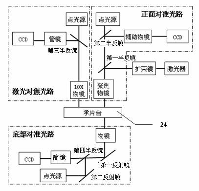
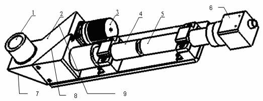
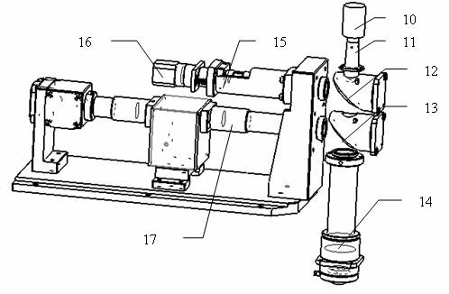
[0021] Embodiment 1: see figure 1 ~Figure 7, the LED (light-emitting diode) laser scribing machine processing visual device has a front alignment optical path coaxial with the laser processing optical path, which is used for the backside identification and positioning of transparent wafers and real-time monitoring of processing, and the front alignment optical path The focusing objective lens (14), the first half mirror (13), the second half mirror (12), the auxiliary objective lens (15) and the CCD camera (16) are installed sequentially from bottom to top, and the laser beam passes through the first half mirror The mirror (13) is coaxially coupled into the front alignment optical path; a bottom alignment optical path coaxial with the laser processing optical path is used for front identification and positioning of special roughened wafers, and the bottom alignment optical path is sequentially installed with objective lenses from top to bottom (1), the first mirror (7), the fo...


PUM

PropertyMeasurementUnit
reflectanceaaaaaaaaaa

Abstract

The invention provides a processing visual device for a light-emitting diode (LED) laser cutting-up machine and relates to the technical field of laser cutting-up machines. The processing visual device mainly comprises a front alignment optical path and a bottom alignment optical path; the front alignment optical path is coaxial with a laser processing optical path and used for identifying and positioning the back of a transparent wafer and monitoring processing in real time; the bottom alignment optical path is coaxial with the laser processing optical path and used for identifying and positioning the front of a special coarsened wafer; and a bottom alignment lens is arranged at the bottom of a wafer chuck (24) and is coaxial with the front alignment lens; and the wafer is arranged on the wafer chuck (24) with an upward back. The front alignment of the wafer can be realized, the cutting-up process requirements of the coarsened wafer can be met in a mode of back cutting-up of the wafer, and the identification and alignment, and scratch monitoring of different wafers can be performed so as to contribute to improving production quality and automation degree. The wafer can be accurately focused by a laser focusing optical path and the cost is relatively low.

Description

[0001] technical field [0002] The invention relates to the technical field of laser scribing machines, in particular to a visual device of a light-emitting diode laser scribing machine. Background technique [0003] Global demand for high-brightness blue LEDs (light-emitting diodes) is driving the continuous development of new production processes. One area that is booming in particular is the die separation process. As an emerging alternative method for slitting blue LEDs, UV laser scribing significantly increases yield and production capacity and reduces equipment operation and maintenance costs compared to traditional mechanical separation methods. The blue LED substrate material sapphire wafer is extremely hard, transparent, and expensive. In order to reduce material costs, the miniaturization of crystal grains and extremely narrow scribe grooves have become the trend; in order to improve luminous efficiency, wafer coating and roughening have become the mainstream. ...

Claims


Application Information

Patent Timeline
Patent Type & Authority Applications(China)
IPC IPC(8): B23K26/02B23K26/42B23K26/03B23K26/046B23K26/36
Inventor 高爱梅
Owner THE 45TH RES INST OF CETC
Why Eureka
Try Eureka