

Optical microscopy-atomic force microscopy double-probe imaging method and device
A technique of atomic force microscopy and optical microscopy, which is applied in measuring devices, scanning probe microscopy, and material analysis through optical means, can solve problems such as the inability to achieve direct and real-time observation and image acquisition, and achieve structural The effect of simplicity and easy technical conditions
Inactive Publication Date: 2011-06-15
ZHEJIANG UNIV
View PDF5 Cites 14 Cited by
- Summary
- Abstract
- Description
- Claims
- Application Information
AI Technical Summary
Problems solved by technology
However, due to the limitation of light wavelength and diffraction limit, the resolution of traditional far-field optical microscope can only reach the half-wavelength order of visible light (380-780nm), that is, about 0.2mm
The micro-nano detection technologies developed in recent decades, mainly represented by scanning probe microscopy (SPM) technologies such as atomic force microscopy (AFM) and scanning tunneling microscopy (STM), have far exceeded the resolution of optical microscopy. What is obtained is a sample image that has been scanned, detected and reconstructed, which cannot achieve direct and real-time observation and image acquisition like an optical microscope
Method used
View moreImage
Smart ImageViewing Examples

Examples
Embodiment Construction
Login to View More PUM
 Abstract
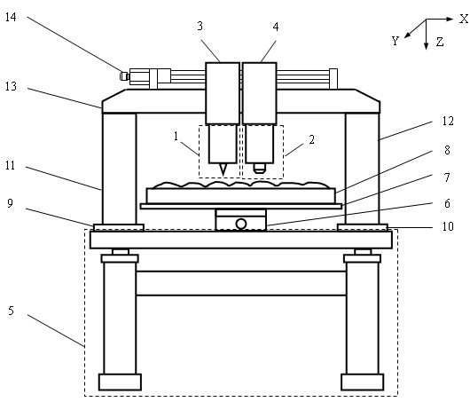
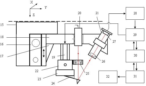
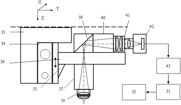
The invention discloses an optical microscopy-atomic force microscopy double-probe imaging method and an optical microscopy-atomic force microscopy double-probe imaging device. The device is provided with a scanner, an atomic force microscopy probe, an optical microscopy probe, a charge coupled device (CCD) detection probe, a data image acquisition system, a Z direction moving mechanism, an XY stepping moving mechanism and an open type large sample platform, wherein the scanner consists of a laser, a micro lens, single-pipe piezoelectric ceramics and a micro cantilever probe; the atomic force microscopy probe comprises a position sensitive detection unit, a photoelectric detection and feedback measurement control system and the like; and the optical microscopy probe consists of a micro objective group and a micro ocular group. An optical microscopy-atomic force microscopy double-probe system provided by the invention can simultaneously solve the problems of the observation of real-time optical microscopy in a wide range and the observation and the measurement of local high-resolution nano structures and performance.
Description
An optical microscope-atomic force microscope dual-probe imaging method and device technical field The invention relates to an optical microscope-atomic force microscope dual-probe imaging method and device. It is used for simultaneous large-scale real-time optical microscopic observation of samples and observation and measurement of high-resolution nanostructures in local areas. Background technique An important trend of science and technology is the rapid development in the direction of small size, large capacity, high speed and low energy consumption. Human exploration of the microcosm has gradually extended from micro-technology to nano-technology, thus promoting the progress of the national economy and human society. Micro-nano technology is the core technology that is planned and developed by major countries in the new century. With the rapid development of micro-nano technology, the requirements for micro-nano microscopic inspection are also getting higher and highe...
Claims
Login to View More Application Information
Patent Timeline
 IPC IPC(8): G01Q60/02G01N21/84
Inventor张冬仙李方浩吴兰章海军
OwnerZHEJIANG UNIV