Method for cutting LED chip

A technology of LED chips and cutting methods, which is applied to fine working devices, electrical components, circuits, etc., can solve the problems of destroying the light-emitting area, reducing the area of ​​the light-emitting area, affecting product quality, etc., and achieves the goal of simple process and increased chip production capacity Effect

Inactive Publication Date: 2011-06-15
Shandong Huaguang Optoelectronics Co. Ltd.
View PDF4 Cites 20 Cited by
  • Summary
  • Abstract
  • Description
  • Claims
  • Application Information

AI Technical Summary

Problems solved by technology

However, there are some troublesome problems in this cutting method: some semiconductor materials are physically brittle, which makes them easier to break during processing; after saw blade cutting, edge chipping, chipping, burrs, etc. , which seriously affects product quality; saw blade cutting takes a lot of time, and the production efficiency is low; the LED light-emitting area is 1/20 to 1/3 away from the chip surface, an

Method used


Image

  • Method for cutting LED chip
  • Method for cutting LED chip
  • Method for cutting LED chip

Examples


Embodiment Construction

[0017] The LED chip cutting method of the present invention will be described in detail below with reference to the accompanying drawings, taking gallium arsenide LED chip cutting as an example.

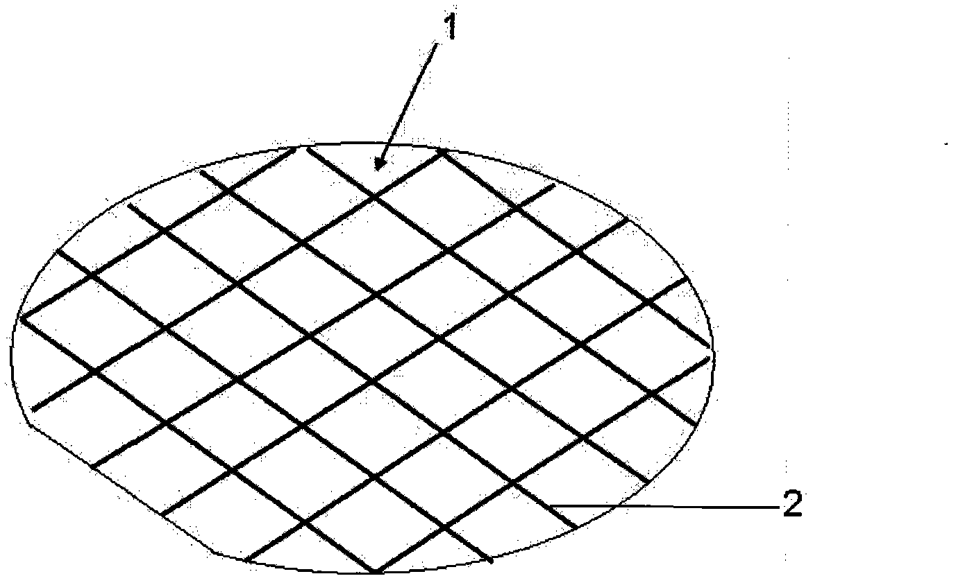
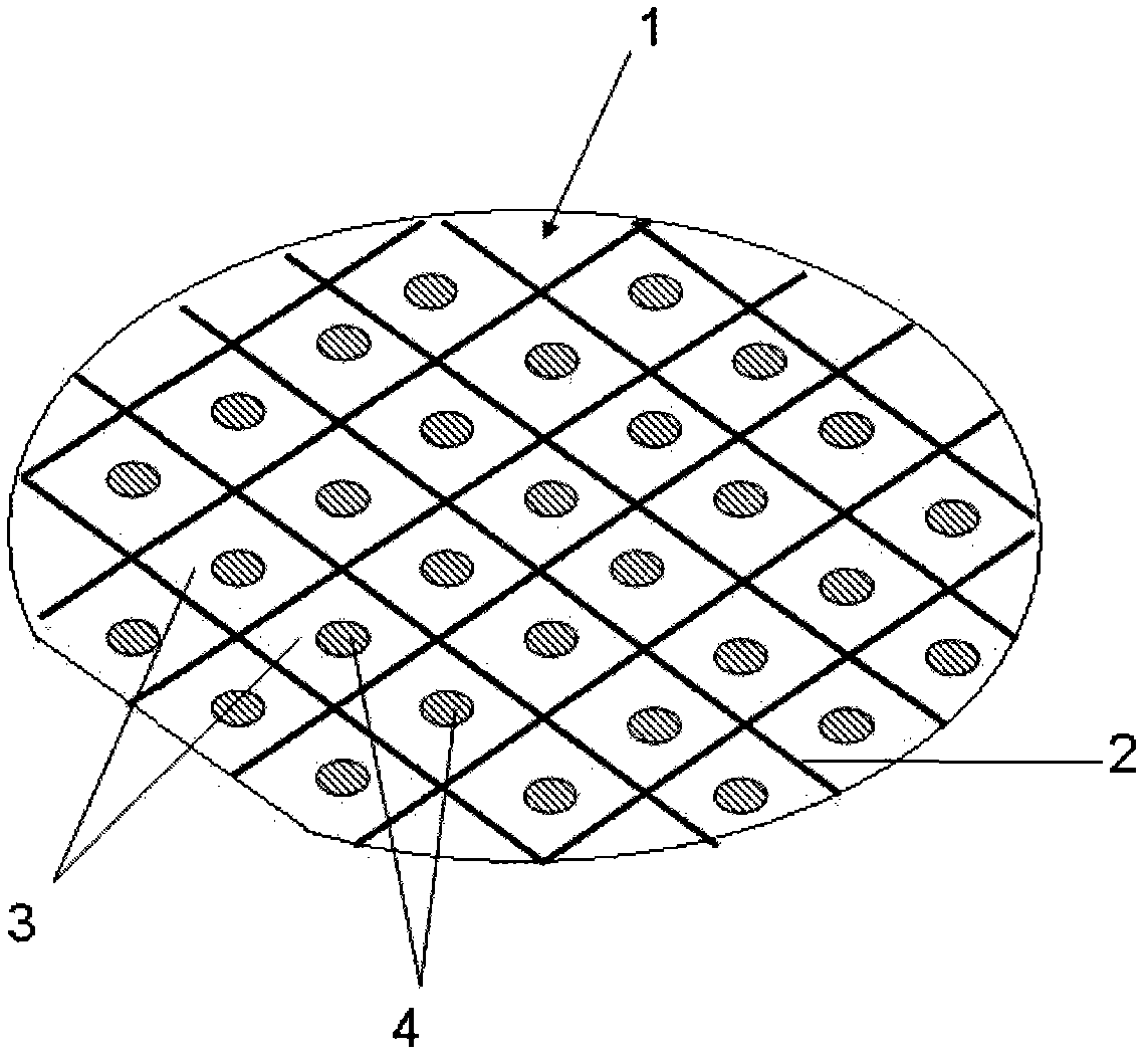
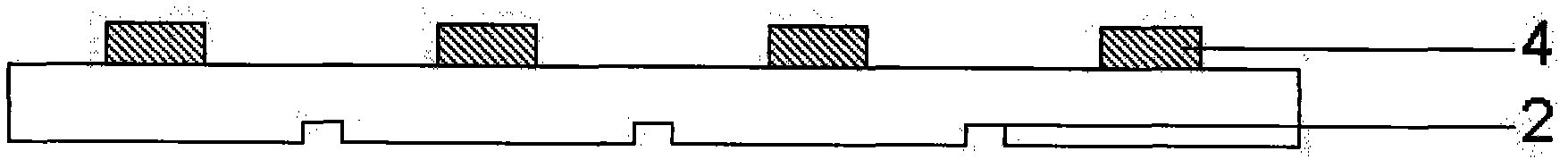
[0018] 1 SMT: Paste the front side (P side) of the gallium arsenide chip 1 on a piece of blue film so that the back side (N side) faces up, and then put the chip together with the blue film on the saw blade carrier On the platform, it is fixed by suction pump;

[0019] 2. Saw blade: After setting the cutting range, cutting depth, cutting speed and chip size and other parameters, start sawing the blade. The saw blade is performed on the back (N side) of the gallium arsenide chip 1, and the cutting depth is set at 1% of the chip thickness. / 6--2 / 3. In this embodiment, the gallium arsenide chip 1 has a thickness of 100 μm, a single chip size of 203 μm, a cutting depth of 40 μm, a cutting period of 203 μm, and a cutting position in the middle of the electrodes. Gallium arsenide chip 1 ...


PUM


Abstract

The invention provides a method for cutting an LED (Light Emitting Diode) chip, which comprises the steps of: on the back face of the chip, sawing along the middle position of two electrodes on the front face, wherein the sawing depth is 1/6 to 2/3 of the thickness of the chip, and then splitting the chip on the front face of the chip along the sawing mark by using a splitter. The method is simple in process and free from the manufacturing of a scribing slot and adopts the manner of sawing on the back face and splitting on the front face so that each side on the front face of the chip only loses the area as large as 1 micron to 5 microns of splitting width, more tube cores can be formed on each chip by splitting so as to increase the chip productivity remarkably, the chip is free from edge breaking, corner breaking, burr, cracking and other problems owing to the manner of sawing on the back face and splitting on the front face as well as incomplete sawing on the back face, and simultaneously, the method is free from the problems of pollution, arsenic evaporation and arsenic oxides and the like.

Description

technical field [0001] The invention relates to a method for cutting LED (light-emitting diode) chips, including gallium arsenide, gallium phosphide, and silicon light-emitting diode chips, and belongs to the technical field of semiconductor chip cutting. Background technique [0002] In the LED chip manufacturing process, cutting is a very important link. The purpose of cutting is to divide the electrodes and connected chips into independent chips one by one. For LED chips, there are currently two cutting processes: saw blade cutting and laser cutting. The traditional and most widely used cutting method in the industry is saw blade cutting. [0003] Saw blade cutting is to use a high-speed rotating saw blade to completely saw (cut through) the chip into a single die according to the set program. Saw cutting technology has been quite mature, and it is still the mainstream technology for gallium arsenide chip cutting. However, there are some troublesome problems in this cu...

Claims


Application Information

Patent Timeline
IPC IPC(8): H01L33/00H01L21/78B28D5/00
Inventor 张秋霞任忠祥夏伟徐现刚
Owner Shandong Huaguang Optoelectronics Co. Ltd.
Why Eureka
Try Eureka