Making method for printed-circuit boards and palladium removing device for printed-circuit boards

A technology for printed circuit boards and manufacturing methods, which is applied in the field of palladium removal for printed circuit boards and the production of printed circuit boards. It can solve the problems of sinking nickel and gold, affecting the reliability of HDI boards, etc., and achieve the effect of improving performance.

Inactive Publication Date: 2011-06-22
PEKING UNIV FOUNDER GRP CO LTD +1
View PDF0 Cites 8 Cited by
  • Summary
  • Abstract
  • Description
  • Claims
  • Application Information

AI Technical Summary

Problems solved by technology

[0002] In the field of high density interconnection (HDI) production, the surface treatment is mainly electroless nickel-gold, because when the metallized hole (Plated through hole, PTH) is formed, the substrate hole wall is adsorbed A layer of colloidal palladium, when the dry film is applied after a comprehensive copper plating, the corresponding non-conducting holes (holes whose walls are not plated with metal and are used for mechanical installation or mechanically fixed components) are also covered by the dry film together, so After the second copper plating and second etching, although the copper in each non-conducting hole (None plated through hole, NPTH for short) has been completely etched away, the palladium adsorbed on the hole wall substrate before copper plating cannot If it is removed, it will cause the non-conducting hole to sink with nickel and gold during the chemical immersion of nickel and gold, which will affect the reliability of the HDI board.

Method used


Image

  • Making method for printed-circuit boards and palladium removing device for printed-circuit boards
  • Making method for printed-circuit boards and palladium removing device for printed-circuit boards

Examples


Embodiment 1

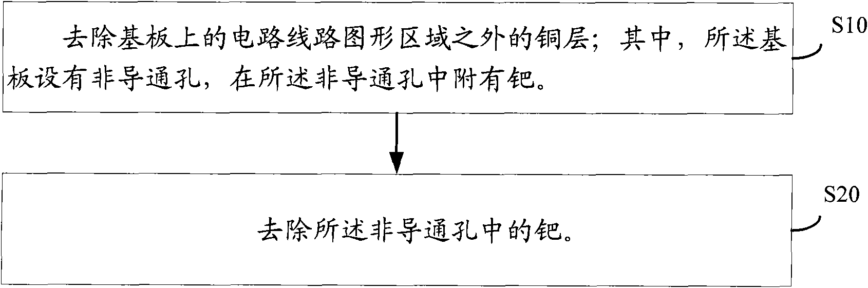
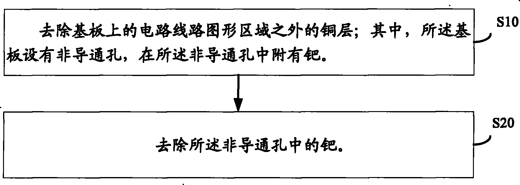
[0017] This embodiment provides a method for manufacturing a printed circuit board. Such as figure 1 As shown, a method for manufacturing a printed circuit board includes:

[0018] S10: removing the copper layer outside the circuit pattern area on the substrate; wherein, the substrate is provided with a non-conducting hole, and palladium is attached to the non-conducting hole;

[0019] S20: removing palladium in the non-conducting holes.

[0020] Wherein, removing the copper layer outside the circuit pattern area on the substrate specifically includes: removing the copper layer outside the circuit pattern area through an etching process. In this embodiment, a horizontal alkaline etching machine is used to perform etching using an ammonium chloride etching solution. Among them, the upper pressure of the etching section of the horizontal alkaline etching machine is 2.0-3.0Kgf, the lower pressure of the etching section is 1.1-1.5Kgf, the chloride ion concentration is controlle...

Embodiment 2

[0039] This embodiment provides a method for removing palladium for manufacturing printed circuit boards, the method can remove palladium in non-conducting holes of the circuit board, and can improve the performance of the circuit board.

[0040] In order to solve the above technical problems, the present invention adopts the following technical solutions:

[0041] A method for removing palladium used for manufacturing printed circuit boards. The palladium removing agent used for palladium removal is a mixed solution of hydrochloric acid solution and thiourea solution. Wherein, the hydrochloric acid solution in the mixed solution is 16-20 g / L of hydrochloric acid with a mass percent content of 37%, and the concentration of the thiourea solution is 60-80 g / L.

[0042] Further, in the mixed solution, the mass ratio of the hydrochloric acid solution and the thiourea solution is 1:3.8.

[0043] Furthermore, the working temperature of the mixed solution is 20-40°C.

[0044] In th...


PUM


Abstract

The invention discloses a making method for printed-circuit boards, comprising the following steps of: removing a copper layer outside a circuit graphic region on a substrate, wherein the substrate is provided with a non-through hole which is internally attached with palladium; and removing palladium in the non-through hole. The invention further discloses a palladium removing device for the printed-circuit boards; during removing palladium, a palladium-removing agent is a mixed solution of a hydrochloric acid solution and a thiocarbamide solution. The invention can be used for making the printed-circuit boards.

Description

technical field [0001] The invention relates to a circuit board, in particular to a method for manufacturing a printed circuit board and a palladium removal method for the printed circuit board. Background technique [0002] In the field of high density interconnection (HDI) production, the surface treatment is mainly electroless nickel-gold, because when the metallized hole (Plated through hole, PTH) is formed, the substrate hole wall is adsorbed A layer of colloidal palladium, when the dry film is applied after a comprehensive copper plating, the corresponding non-conducting holes (holes whose walls are not plated with metal and are used for mechanical installation or mechanically fixed components) are also covered by the dry film together, so After the second copper plating and second etching, although the copper in each non-conducting hole (None plated through hole, NPTH for short) has been completely etched away, the palladium adsorbed on the hole wall substrate before ...

Claims


Application Information

Patent Timeline
Patent Type & Authority Applications(China)
IPC IPC(8): H05K3/00H05K3/22
Inventor 徐朝晖
Owner PEKING UNIV FOUNDER GRP CO LTD
Why Eureka
Try Eureka