

Photoetching machine projection objective lens wave aberration field measurement method
A technology of projection objective lens and wave aberration, which is applied in microlithography exposure equipment, testing optical performance, exposure device of photo-plate making process, etc. It can solve the problem that the measurement accuracy of TAMIS technology cannot meet the requirements, the number of Zernike coefficients is limited, and the measurement speed is slow and other problems, to achieve the effect of improved detection speed, improved measurement accuracy, and simple measurement method
- Summary
- Abstract
- Description
- Claims
- Application Information
AI Technical Summary
Problems solved by technology
Method used
Image


Examples
Embodiment Construction
[0036] In the following, preferred embodiments according to the present invention will be described in detail with reference to the accompanying drawings. For the convenience of describing and highlighting the present invention, relevant components existing in the prior art are omitted from the drawings, and the description of these known components will be omitted.
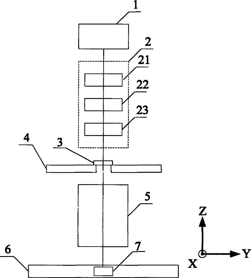
[0037] figure 1 Shown is a schematic structural diagram of the on-site measurement system for wave aberration of the projection objective lens of a photolithography machine according to the present invention. The system includes a light source 1 for generating an illumination beam; an illumination system 2 for adjusting the beam waist size, light intensity distribution, partial coherence factor and illumination mode of the light beam emitted by the light source; a test mask 3 capable of carrying and accurately positioned Mask table 4; a projection objective lens 5 capable of imaging the graphics on the test mask...
PUM
 Abstract
Description
Claims
Application Information