Test structure and test method for coupling capacitance of metal redundant fillers in integrated circuit

A technology for testing structure and coupling capacitance, which is applied in circuits, semiconductor/solid-state device testing/measurement, electrical components, etc. It can solve the problems of error between simulation results and actual values, time-consuming simulation calculation, complex circuit model, etc., and achieve simplification. Measuring the effect of the question

Active Publication Date: 2011-07-20
INST OF MICROELECTRONICS CHINESE ACAD OF SCI
View PDF0 Cites 21 Cited by
  • Summary
  • Abstract
  • Description
  • Claims
  • Application Information

AI Technical Summary

Problems solved by technology

However, there are many defects in the use of EDA tool software. For example, the internal circuit model of the software is complex, and it takes a lot of simulation and calculation time for the layout of complex structures, and there is a certain degree of error between the simulation results and the actual values.

Method used


Image

  • Test structure and test method for coupling capacitance of metal redundant fillers in integrated circuit
  • Test structure and test method for coupling capacitance of metal redundant fillers in integrated circuit
  • Test structure and test method for coupling capacitance of metal redundant fillers in integrated circuit

Examples


Embodiment Construction

[0040] The technical solution of the present invention will be described in detail below in conjunction with the accompanying drawings and a specific embodiment.

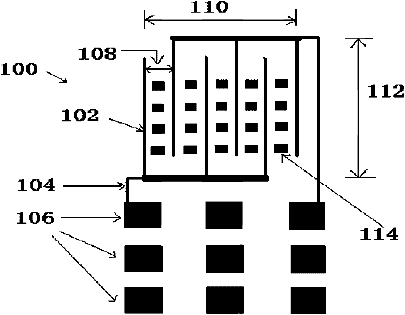
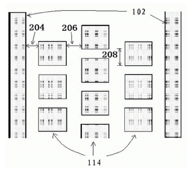
[0041] see figure 1 The invention provides a test structure for the coupling capacitance of an integrated circuit metal redundant filling, which is used for measuring the coupling capacitance of the integrated circuit structure. The test structure of this embodiment is a multi-layer structure composed of several test metal layers, figure 1 is a schematic diagram of a single-layer test metal layer. The test metal layer is set on the medium 100, and its main body is a square copper wire array to be tested, and the array is formed by arranging a plurality of copper wires to be tested 102 parallel to each other, as shown in the figure, odd-numbered columns in the array ( figure 1 The copper wires 102 to be tested in columns 1, 3, and 5) are connected by horizontal leads inside the array to form a comb-shaped copper wi...


PUM


Abstract

The invention relates to a test structure and a test method for coupling capacitance of metal redundant fillers in an integrated circuit. In the process of manufacturing the integrated circuit, redundant metal is often filled into a layout to improve the planarization effect, but the coupling capacitance is influenced by the redundant metal greatly. Therefore, based on the condition, the invention provides a test structure for the coupling capacitance of the metal redundant fillers and a test method using the test structure. The test structure comprises test metal layers formed by media, a copper wire array to be tested, peripheral leads and test pins. In the test structure, the coupling capacitance of the metal redundant fillers can be measured effectively by the multi-layer test structure, the influence on the coupling capacitance can be compared for different types of metal redundant filling structures, and the measurement of multilayer interconnection wires can be simplified by arranging the metal redundant fillers for improving the chemical mechanical planarization (CMP) effect in a coupling capacitance actual test structure additionally and selecting the test structure of anappropriate size and designing a special pin and lead structure.

Description

technical field [0001] The invention relates to the technical field of integrated circuit manufacturing technology and layout design, in particular to a testing structure and method for coupling capacitors of integrated circuit metal redundant fillers. Background technique [0002] The integrated circuit (Integrated Circuit, IC) manufacturing technology develops at a speed of doubling the integration level every 18 months according to Moore's Law. As device feature sizes shrink, the effects of parasitic parameters become more pronounced. Parasitic parameters are essentially caused by the introduction of a new circuit structure. For example, if a metal line is placed next to another metal line, there will be parasitic effects. Especially in the current circuit with relatively high frequency and high wiring density, the problem of parasitic effects seriously affects the timing convergence and signal integrity of the circuit. Therefore, in the process of integrated circuit de...

Claims


Application Information

Patent Timeline
Patent Type & Authority Applications(China)
IPC IPC(8): H01L23/544H01L21/66
CPCH01L2924/0002
Inventor 王强陈岚阮文彪李志刚杨飞周隽雄叶甜春
Owner INST OF MICROELECTRONICS CHINESE ACAD OF SCI
Why Eureka
Try Eureka