High-voltage insulation type LDNMOS (laterally diffused metal oxide semiconductor) device and manufacture method thereof

A high-voltage isolation and high-voltage technology, which is applied in semiconductor/solid-state device manufacturing, electric solid-state devices, semiconductor devices, etc., to achieve the effects of reducing source-drain on-resistance, improving device breakdown, and flattening electric field distribution

Active Publication Date: 2011-07-27
SHANGHAI HUAHONG GRACE SEMICON MFG CORP
View PDF3 Cites 17 Cited by
  • Summary
  • Abstract
  • Description
  • Claims
  • Application Information

AI Technical Summary

Problems solved by technology

The integration of devices with different structures and requirements brings challenges and opportunities to the overall process integration

Method used


Image

  • High-voltage insulation type LDNMOS (laterally diffused metal oxide semiconductor) device and manufacture method thereof
  • High-voltage insulation type LDNMOS (laterally diffused metal oxide semiconductor) device and manufacture method thereof
  • High-voltage insulation type LDNMOS (laterally diffused metal oxide semiconductor) device and manufacture method thereof

Examples


Embodiment Construction

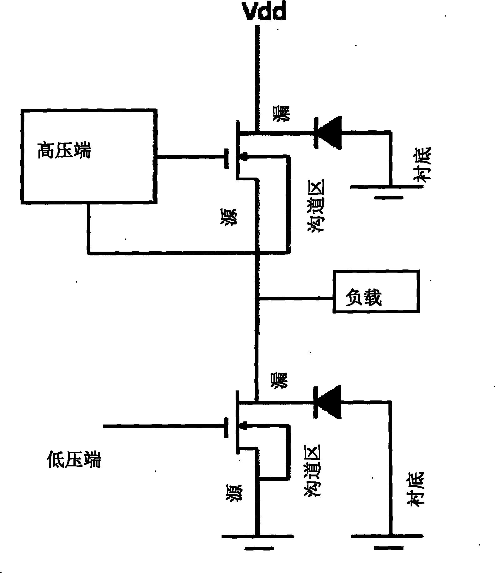
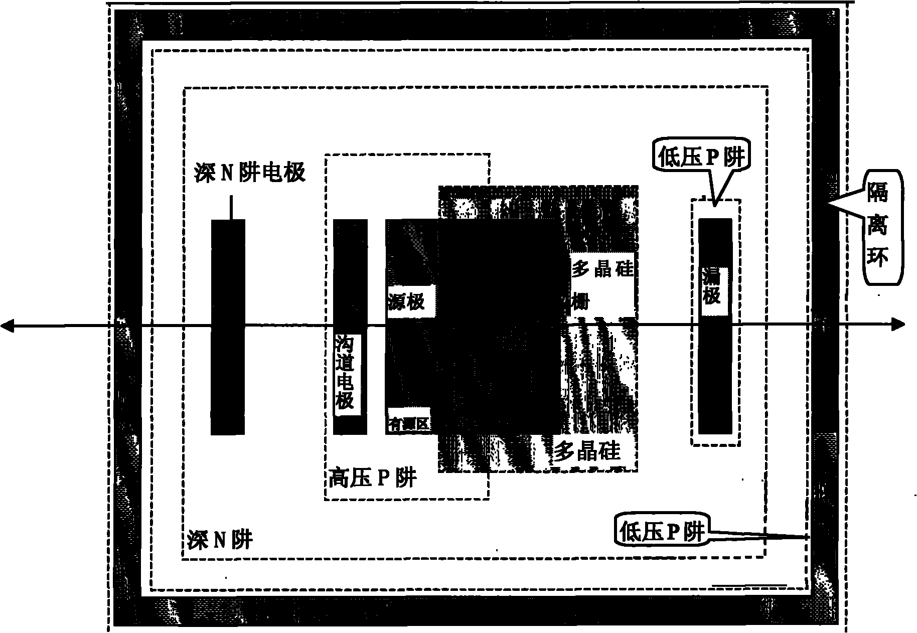
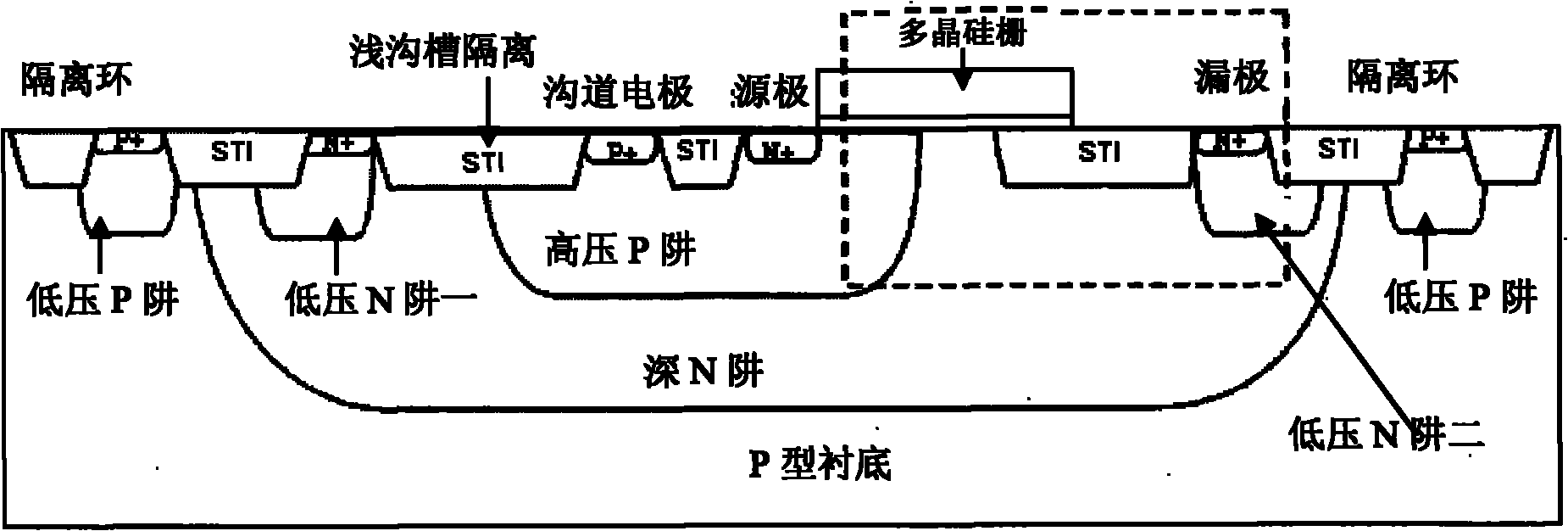
[0032] Such as Figure 6 As shown, it is a plan view of a high voltage isolation type LDNMOS device of the present invention; as Figure 7 Shown is a cross-sectional view of the high-voltage isolation LDNMOS device of the present invention. The high-voltage isolated LDNMOS device provided by the present invention includes: a P-type substrate, and the substrate electrode is drawn out through a low-voltage P well formed in the substrate and then made into a P+ ohmic contact, and the substrate electrode forms an isolation ring (Isolation Ring) ; a deep N well, the electrode of the deep N well is drawn out through a low-voltage N well as an N+ ohmic contact; a channel region is formed by a high-voltage P well formed in the deep N well, and is drawn out through a P+ ohmic contact A channel electrode; a source region, composed of an N+ doped region formed in the channel region, directly making an ohmic contact to lead out the source; a drain region, formed in a low-voltage N well 2 f...


PUM


Abstract

The invention discloses a high-voltage insulation type LDNMOS (laterally diffused metal oxide semiconductor) device, which comprises a deep N well, a channel region, a source region, a drain region, and a polysilicon fence. Shallow channel insulation is formed in the deep N well between the drain region and the channel region; a high voltage P well and a low voltage N well are formed in the deep N well at the bottom part of the shallow channel insulation; and a drift region of the device consists of the deep N well between the drain region and the channel region, the low voltage N well and the high voltage P well. The invention also discloses a manufacture method for the high-voltage insulation type LDNMOS (laterally diffused metal oxide semiconductor) device. The invention can be realized by only alternating the domains of a high voltage P well of a current high-voltage insulation type LDNMOS and a low voltage N well of a current SONOS (silicon oxide nitride oxide semiconductor) without needing to add a photomask; therefore, the puncturing characteristic of the high voltage device and the on resistance characteristic of the source and the drain can be optimized simultaneously, and the cost can be greatly reduced.

Description

technical field [0001] The invention relates to the field of semiconductor integrated circuits, in particular to a high-voltage isolation LDNMOS device, and also relates to a manufacturing method of the high-voltage isolation LDNMOS device. Background technique [0002] Such as figure 1 Shown is a schematic diagram of a working circuit of an existing high-voltage isolated LDNMOS device (Isolated HV LDNMOS). Due to application requirements, when the device is turned on, the source and channel of the high-voltage LDNMOS device will be in a high potential state. In order to avoid the impact of high voltage on the substrate, an N-type well is usually used to wrap the entire device, which is called an isolated LDNMOS device (Isolated LDNMOS). [0003] Such as figure 2 and image 3 As shown in FIG. 2 , they are respectively the planar structure diagram and the cross-sectional diagram of the existing high-voltage isolated LDNMOS device. Existing high-voltage isolation LDNMOS ...

Claims


Application Information

Patent Timeline
Patent Type & Authority Applications(China)
IPC IPC(8): H01L29/78H01L29/06H01L27/04H01L21/336H01L21/77
Inventor 陈华伦陈瑜熊涛陈雄斌罗啸
Owner SHANGHAI HUAHONG GRACE SEMICON MFG CORP
Why Eureka
Try Eureka