Flip-chip construction maintaining solder positioning

A flip-chip packaging, welding positioning technology, applied in electrical components, electrical solid devices, circuits, etc., can solve the problems of electrical connection failure, general products do not have suitable structures, and the cost of flip-chip bonding machines is expensive. The effect of reliability

Inactive Publication Date: 2011-08-03
POWERTECH TECHNOLOGY
View PDF3 Cites 14 Cited by
  • Summary
  • Abstract
  • Description
  • Claims
  • Application Information

AI Technical Summary

Problems solved by technology

Therefore, in the flip-chip bonding process, the machine identification system will be used to find the reference mark for alignment calibration. In this way, a machine with very accurate alignment (allowable displacement tolerance within 25 microns) will be required to achieve The wafer 110 and the substrate 120 are successfully bonded, but the cost of the high-precision flip-chip bonding machine itself is quite expensive
In addition, even with precise bonding, the transfer process to the reflow step after bonding the wafer 110 and the substrate 120, the vibration of the tool changeover and the overflow of solder or flux can cause the bumps 112 to be soldered to the wrong pads. 121, it will lead to electrical connection failure, especially when used in MPS-C2 products, there will be a more obvious decline in yield
[0006] It can be seen that the above-mentioned existing flip-chip packaging structure obviously still has inconvenience and defects in structure and use, and needs to be further improved urgently.
In order to solve the above-mentioned problems, the relevant manufacturers have tried their best to find a solution, but for a long time no suitable design has been developed, and the general product has no suitable structure to solve the above-mentioned problems. This is obviously the relevant industry. Urgent problem

Method used


Image

  • Flip-chip construction maintaining solder positioning
  • Flip-chip construction maintaining solder positioning
  • Flip-chip construction maintaining solder positioning

Examples


no. 1 Embodiment

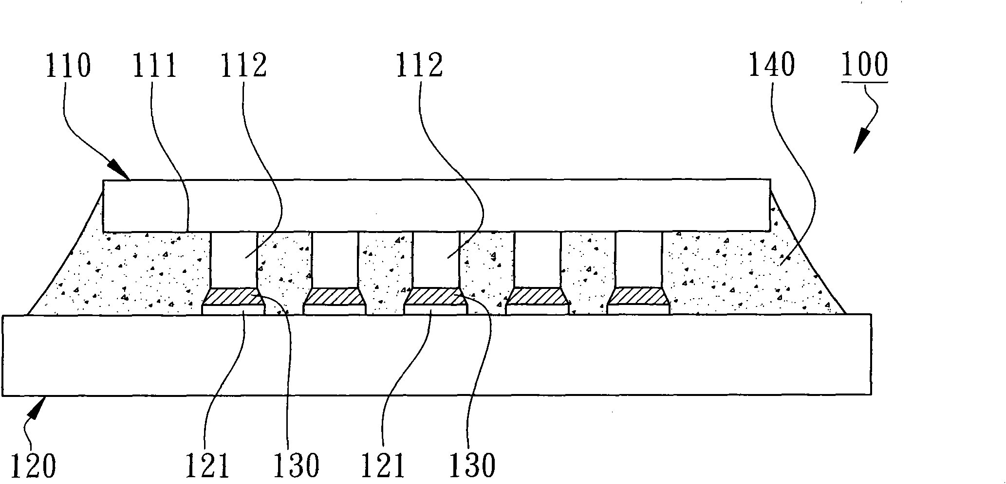
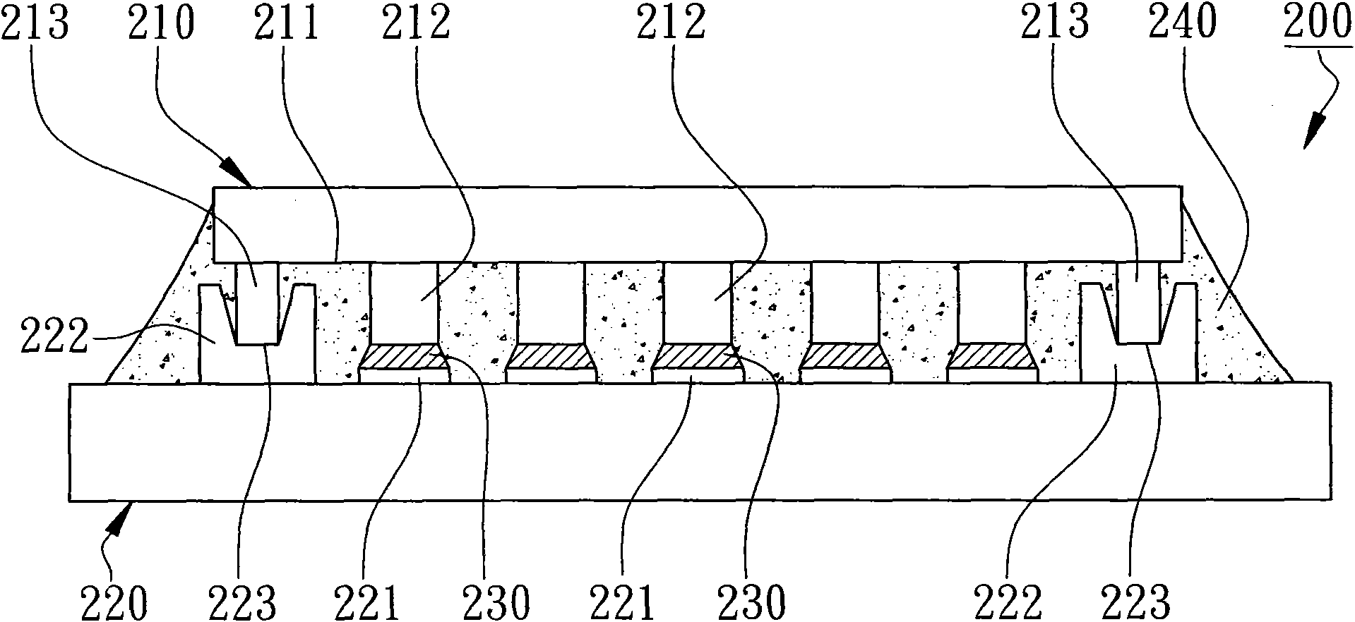
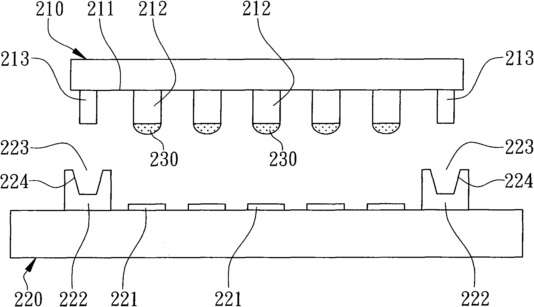
[0054] According to the first embodiment of the present invention, a flip-chip package structure for maintaining soldering positioning is exemplified in figure 2 cross-sectional diagram of Figure 3A to Figure 3C Schematic cross-sectional view of components during flip-chip bonding and Figure 4A and Figure 4B A partial top view of its wafer and substrate is shown. The flip-chip package structure 200 for maintaining soldering position mainly includes a chip 210 and a substrate 220 .

[0055] see figure 2 Shown is a schematic cross-sectional view of a flip-chip package structure for maintaining soldering positioning according to the first embodiment of the present invention. The active surface 211 of the wafer 210 is provided with a plurality of bumps 212 and at least one embossed base mark 213 . In detail, the active surface 211 may additionally be formed with a plurality of solder pads (not shown in the figure) for connecting the bumps 212, and an UBM layer ( not sho...

no. 2 Embodiment

[0072] According to the second specific embodiment of the present invention, another flip-chip package structure for maintaining soldering positioning is illustrated in Figure 7 The cross-sectional diagram of the Figure 8 Schematic cross-section of the component. The main components that are the same as those in the first embodiment will be marked with the same symbols and will not be described in detail again.

[0073] The present invention is not limited to the MPS-C2 product, and can also be used in a flip-chip packaging structure bonded by solder balls. see Figure 7 Shown is a schematic cross-sectional view of another flip-chip package structure for maintaining soldering positioning according to the second embodiment of the present invention. The flip-chip package structure 300 for maintaining soldering position mainly includes a chip 210 and a substrate 220 . The wafer 210 is provided with a plurality of bumps 212 and at least one embossed mark 213 on its active su...


PUM


Abstract

The invention discloses a flip-chip construction which maintains solder positioning. The flip-chip construction mainly comprises a chip and a substrate, wherein a plurality of bumps and at least one convex basic mark are formed on an active surface of the chip; the substrate is provided with a plurality of soldering pads and at least one basic mark seat; the basic mark seat is provided with a concave basic mark pattern which corresponds to the convex basic mark; and when the chip is arranged on the substrate in an alignment mode, the convex basic mark is embedded into the concave basic mark pattern to make the bumps aligned with the soldering pads. Therefore, even if a mechanical alignment error exists, the bumps of the chip can be soldered to the soldering pads of the substrate accurately, and particularly, products which are applied to metal post solder-chip connection (MPS-C2) have a better yield.

Description

technical field [0001] The invention relates to a semiconductor device, in particular to a flip-chip packaging structure for maintaining soldering positioning. Background technique [0002] In the semiconductor industry, the conventional packaging method is to place the chip on the substrate, and then use wire-bond technology to connect the chip and the substrate, and complete the electrical connection relationship between the two. Flip-chip packaging technology (Flip-Chip) is an advanced chip packaging technology. It is different from the previous chip packaging method. It is to set bumps on the active surface of the chip, such as solder bumps or solder balls, and then the chip Turn it over so that the active surface faces the substrate, and use the bump itself to electrically connect the chip and the substrate, thereby shortening the transmission distance between the chip and the substrate, achieving better electrical performance than wire bonding, and gradually becoming p...

Claims


Application Information

Patent Timeline
Patent Type & Authority Applications(China)
IPC IPC(8): H01L23/12H01L23/485
CPCH01L2224/16225H01L2224/32225H01L2224/73204H01L2924/00
Inventor 徐宏欣柯志明
Owner POWERTECH TECHNOLOGY
Why Eureka
Try Eureka