Horizontal light emitting diode and manufacturing method thereof

A technology of light-emitting diodes and manufacturing methods, which is applied in the direction of electrical components, circuits, semiconductor devices, etc., can solve the problems of reduced luminous efficiency, troublesome manufacturing process, and difficult alignment, so as to reduce forward bias voltage, easy manufacture, and increase luminescence benefit effect

Inactive Publication Date: 2011-08-03
HIGH POWER OPTO
View PDF0 Cites 2 Cited by
  • Summary
  • Abstract
  • Description
  • Claims
  • Application Information

AI Technical Summary

Problems solved by technology

However, the P-type ohmic contact metal electrode layer 7 is distributed on the mirror protective layer 8 in a sheet shape, so the position of the P-type ohmic contact metal electrode layer 7 needs to be determined by an alignment technique, and the manufacturing process is rather cumbersome, and When the overall structure is distorted, it will cause more difficulties in alignment. In addition, the P-type ohmic contact metal electrode layer 7 is a light-absorbing material, which will also reduce the overall luminous efficiency.

Method used


Image

  • Horizontal light emitting diode and manufacturing method thereof
  • Horizontal light emitting diode and manufacturing method thereof
  • Horizontal light emitting diode and manufacturing method thereof

Examples


Embodiment Construction

[0015] The detailed content and technical description of the present invention are further described by examples, but it should be understood that the following examples are only for illustrative purposes, and should not be construed as limitations to the implementation of the present invention.

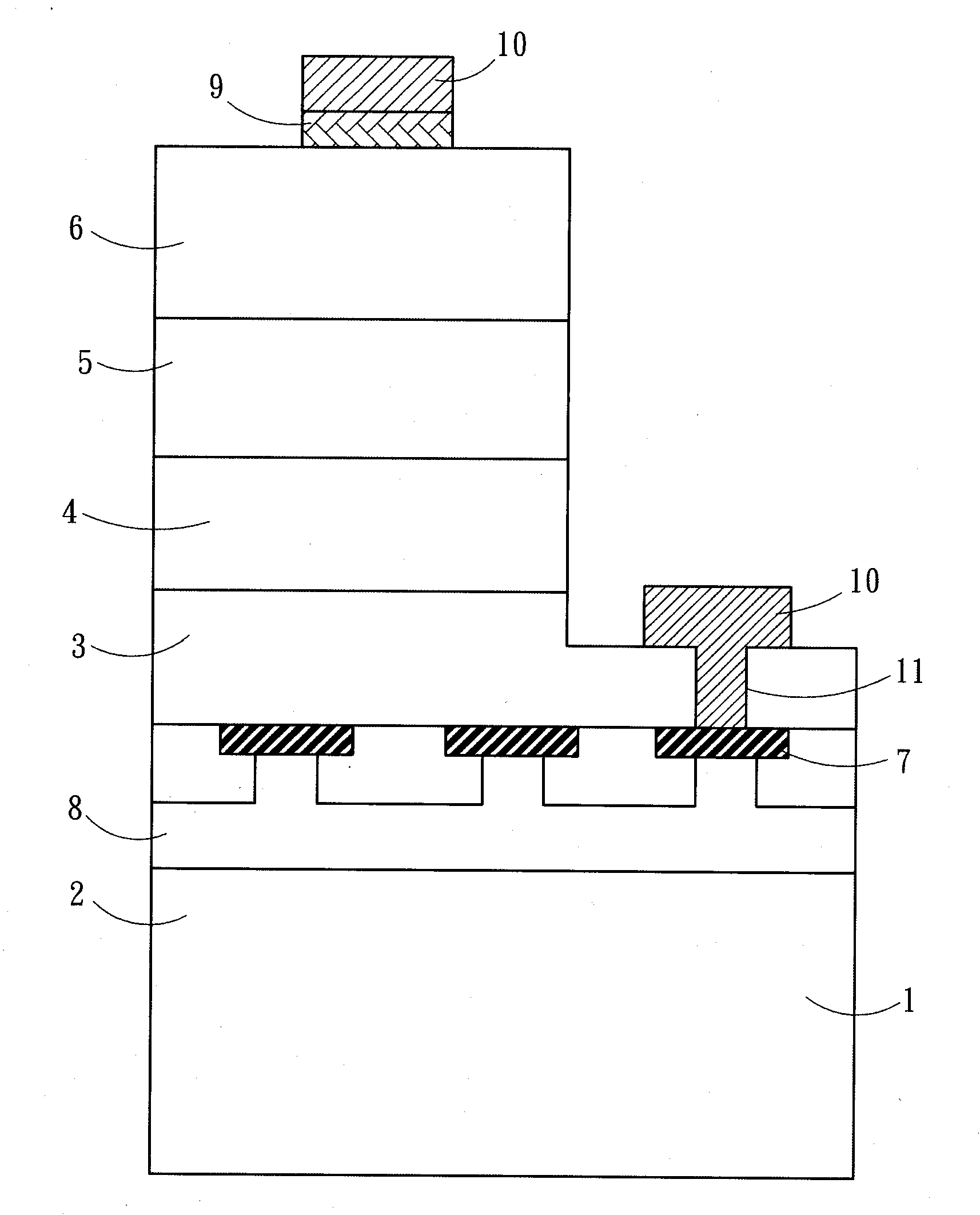
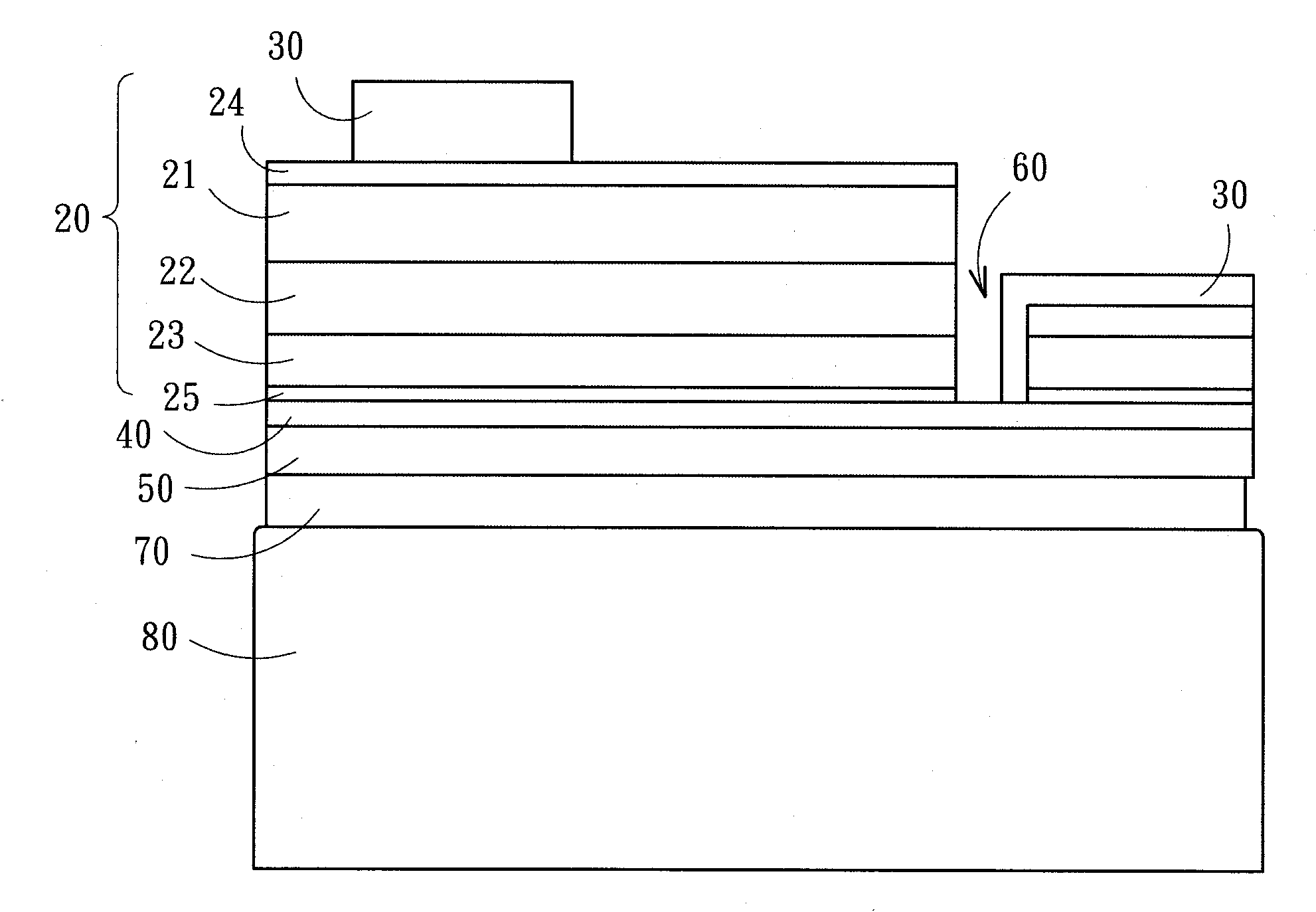
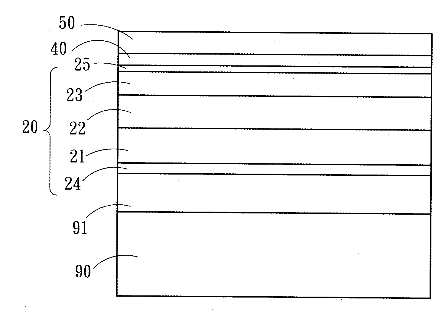
[0016] see figure 2 As shown, it is an embodiment of the present invention, which includes a light-emitting laminated layer 20, a transparent conductive layer 40, a high reflection layer 50, an electrical connection channel 60 and two stitching electrode layers 30, wherein the light-emitting laminated layer 20 may have a first ohmic contact layer 24, an upper cladding layer 21, an active layer 22, a lower cladding layer 23 and a second ohmic contact layer 25 formed in sequence, wherein the active layer 22 is aluminum phosphide Gallium indium epitaxy (AlGaInP) structure or aluminum gallium indium nitride epitaxy structure, and the upper cladding layer 21 can be P-type aluminum galliu...


PUM


Abstract

The invention discloses a horizontal light emitting diode and a manufacturing method thereof. The horizontal light emitting diode comprises a luminous lamination layer, a transparent conductive layer, a high reflection layer, an electrical communicating channel and two nail line electrode layers, wherein the transparent conductive layer covers the luminous lamination layer; the high reflection layer is formed on one side of the transparent conductive layer far from the luminous lamination layer; the electrical communicating channel passes through the luminous lamination layer to the transparent conductive layer; and one of the two nail line electrode layers is arranged on one side of the luminous lamination layer without the transparent conductive layer, the other one is electrically connected with the transparent conductive layer through the electrical communicating channel, and voltage drop is formed between the two nail line electrode layers. The electrical communicating channel can be in contact with the transparent conductive layer without aligning, so that the horizontal light emitting diode can be easily manufactured and forward bias can be reduced; and the transparent conductive layer can be transmitted by light and the light is totally reflected by the high reflection layer, so that the light emitting efficiency can be increased to meet the requirements.

Description

technical field [0001] The invention relates to a light emitting diode, in particular to a horizontal light emitting diode, and also to a manufacturing method of the horizontal light emitting diode. Background technique [0002] A light emitting diode (Light Emitting Diode, LED) is a kind of luminescent light-emitting element. Its light-emitting principle is to apply a current to the III-V compound semiconductor material, and use the combination of electrons and holes in the diode to convert energy into the form of light. , it can emit light when the energy is released, and it will not be as hot as an incandescent bulb after a long time of use. The advantages of light-emitting diodes are small size, long life, low driving voltage, fast response rate, and excellent shock resistance. They can meet the needs of light, thin, and miniaturized equipment, and have become very popular products in daily life. [0003] The current luminous performance and efficiency of light-emitting...

Claims


Application Information

Patent Timeline
Patent Type & Authority Applications(China)
IPC IPC(8): H01L33/38H01L33/46
Inventor 张智松廖田福
Owner HIGH POWER OPTO
Why Eureka
Try Eureka