Method for testing inductance

A technology of inductance and inductance value, applied in the field of microelectronics, can solve the problems that the chip does not meet the actual needs, the parasitic inductance and parasitic resistance cannot be eliminated, and the error is large

Active Publication Date: 2011-08-10
SEMICON MFG INT (SHANGHAI) CORP +1
View PDF4 Cites 7 Cited by
  • Summary
  • Abstract
  • Description
  • Claims
  • Application Information

AI Technical Summary

Problems solved by technology

Since the first scattering parameter S 1 The scattering parameters including the inductance value of the inductor, the scattering parameters corresponding to the parasitic inductance, parasitic resistance and parasitic capacitance on the pad and the lead, and the second scattering parameter S 2 Only the scattering parameters corresponding to the parasitic capacitance on the pad and lead are included, but the parasitic inductance and parasitic resistance on the pad and lead cannot be eliminated
In addition, if a wire material is used to connect the first lead 101 and the second lead 102 to form a chip with a short circuit structure, measure the relevant parameters

Method used


Image

  • Method for testing inductance
  • Method for testing inductance
  • Method for testing inductance

Examples


Embodiment Construction

[0035] In the following description, numerous specific details are given in order to provide a more thorough understanding of the present invention. It will be apparent, however, to one skilled in the art that the present invention may be practiced without one or more of these details. In other examples, some technical features known in the art are not described in order to avoid confusion with the present invention.

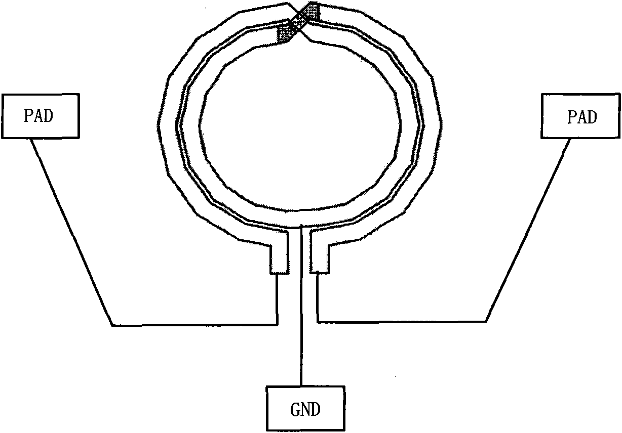
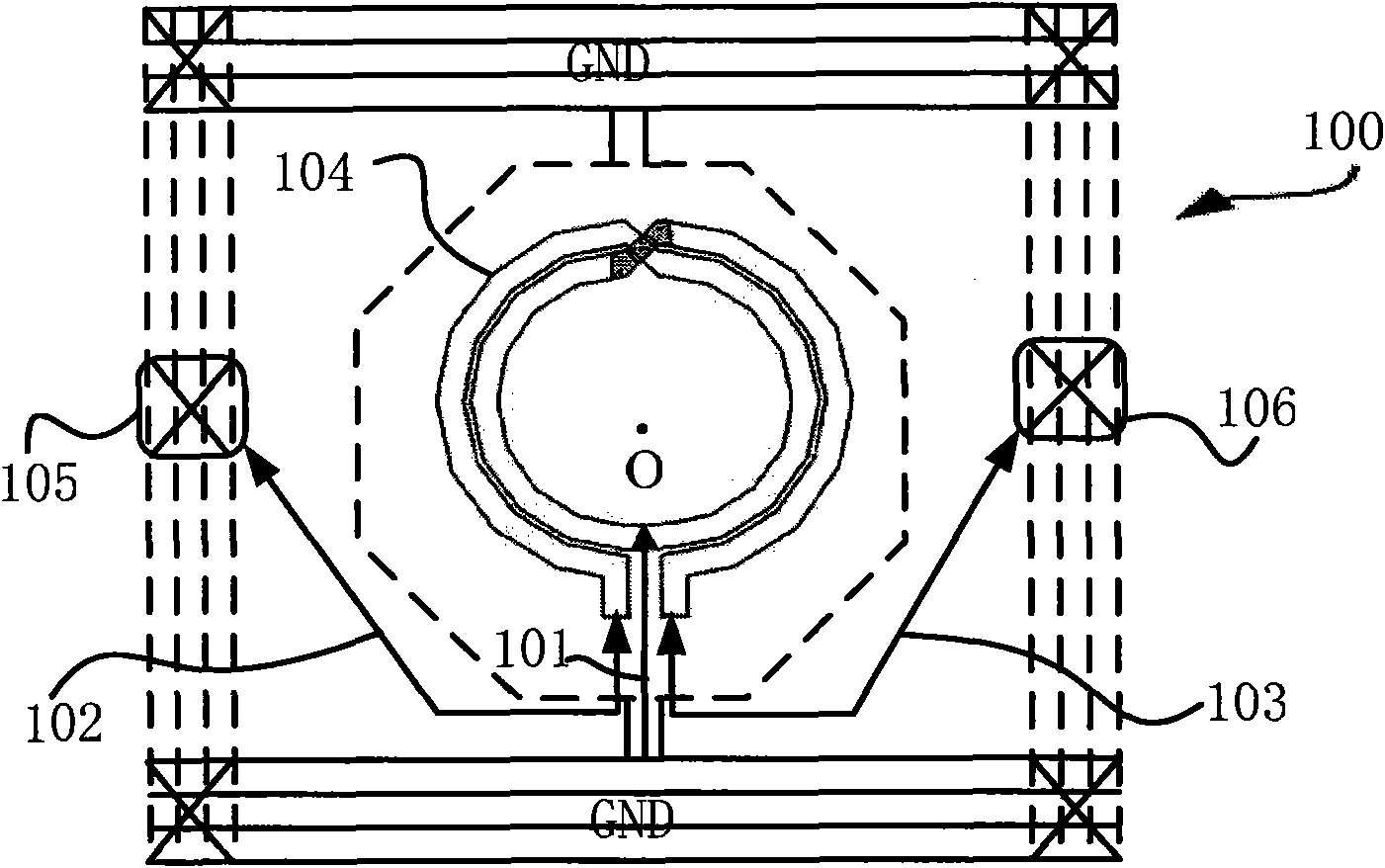
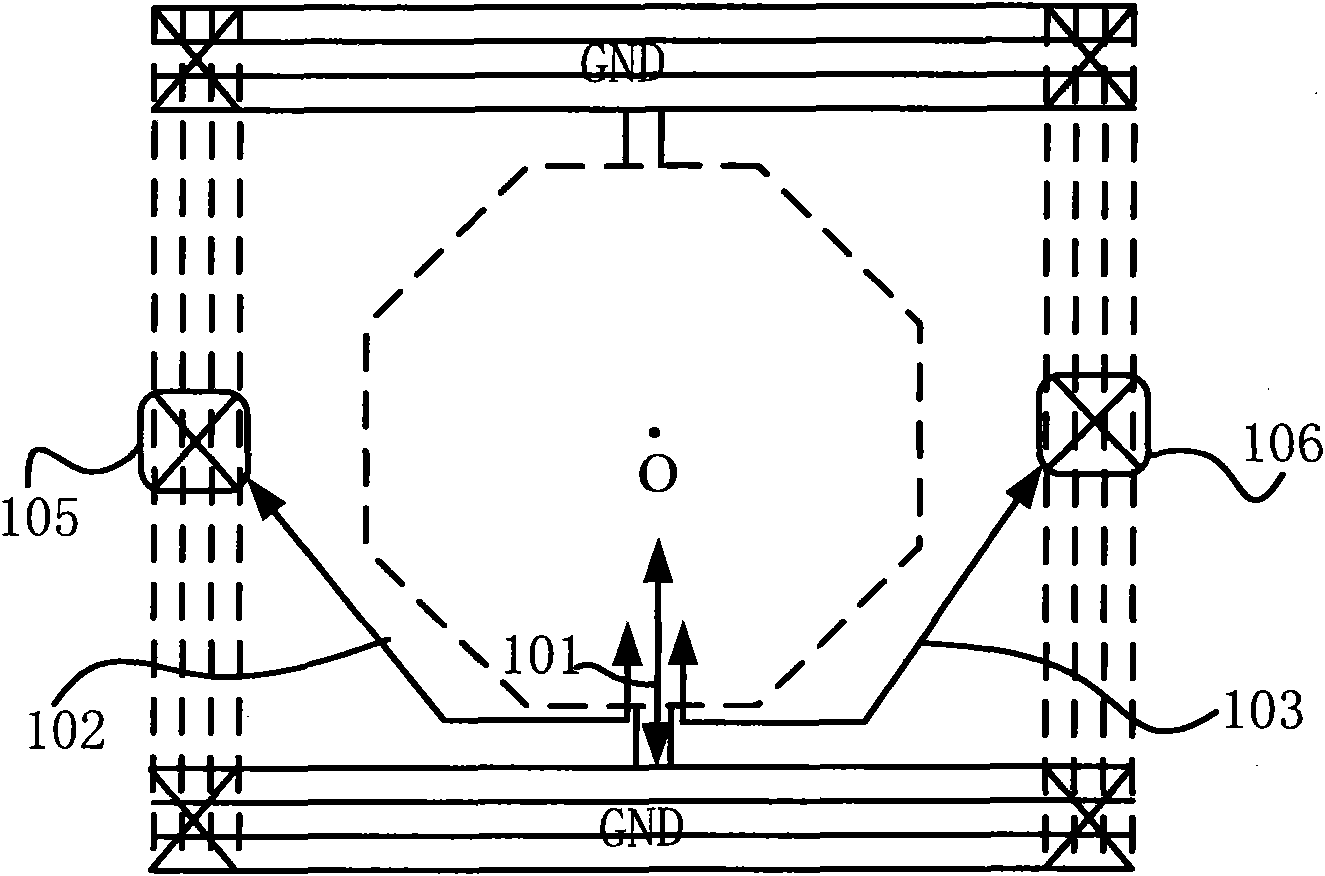
[0036]The present invention provides an improved design method for testing three-terminal differential inductance. Using the method of the present invention is how to accurately measure the inductance value of the inductor, that is, by designing the open circuit structure and short circuit structure, effectively removing the parasitic on the pad and the lead. Capacitance, and can further remove the parasitic inductance and parasitic resistance of the pad and lead, and obtain the test result of the inductance value of the inductor. Based on the test results, a b...


PUM


Abstract

The invention discloses a method for testing inductance. A wafer comprises an inductor arranged on the wafer and an external lead wire connected with the inductor, and the external lead wire comprises a first lead wire for making the inductor grounded, a second lead wire and a third lead wire which are used for making the two ends of the inductor respectively connected with corresponding bonding pads. The method comprises the following steps of: measuring a first parameter containing the inductor and the external lead wire; removing the inductor to obtain an open circuit structure containing the external lead wire; measuring a second parameter of the open circuit structure; mutually connecting the external lead wire of the open circuit structure to form a short circuit structure; measuring a third parameter of the short circuit structure; acquiring a fourth parameter for expressing an inductance value by deducting the second parameter and the third parameter from the first parameter. By the method, the inductance value of a tested inductor is more accurate and the error range is 2 percent.

Description

technical field [0001] The invention relates to the technical field of microelectronics, in particular to a method for testing three-terminal differential inductance. Background technique [0002] In integrated circuits, active devices are very important, but they also include large-area passive devices, including on-chip transmission lines and on-chip inductors. In typical wireless products, inductive components account for less than ten percent of the total components, but they have a significant impact on the overall RF performance. Therefore, the design and analysis of inductance on these passive components has also been extensively studied. Due to the formation of large-scale integrated circuits, spiral inductors are widely used in voltage-controlled oscillators, low-noise amplifiers, power amplifiers, mixers and impedance matching circuits. Since the inductor is a kind of energy storage element, the change of the inductance value of the spiral inductor can usually af...

Claims


Application Information

Patent Timeline
IPC IPC(8): G01R27/26G01R27/02
Inventor 何丹
Owner SEMICON MFG INT (SHANGHAI) CORP
Why Eureka
Try Eureka