SOI-LIGBT (silicon on insulator-lateral insulated gate bipolar transistor) device with split anode structure

An anode structure and anode technology, applied in the direction of semiconductor devices, electrical components, circuits, etc., can solve the problems of slow turn-off time of SOI-LIGBT, increased cost of integrated circuits, large on-resistance, etc., and achieve the elimination of negative differential resistance area, Excellent conduction loss, increase the effect of on-resistance

Inactive Publication Date: 2011-08-10
UNIV OF ELECTRONICS SCI & TECH OF CHINA
View PDF3 Cites 32 Cited by
  • Summary
  • Abstract
  • Description
  • Claims
  • Application Information

AI Technical Summary

Problems solved by technology

The SOI-LIGBT with this structure has a good compromise between speed and on-resistance, but because an external circuit is required to specifically apply a bias voltage to the anode auxiliary gate, and the bias voltage is a floating voltage, it will greatly increase the device and The cost of integrated circuits for device applica...

Method used


Image

  • SOI-LIGBT (silicon on insulator-lateral insulated gate bipolar transistor) device with split anode structure
  • SOI-LIGBT (silicon on insulator-lateral insulated gate bipolar transistor) device with split anode structure
  • SOI-LIGBT (silicon on insulator-lateral insulated gate bipolar transistor) device with split anode structure

Examples


Embodiment Construction

[0018] The present invention will be further described below in conjunction with accompanying drawing.

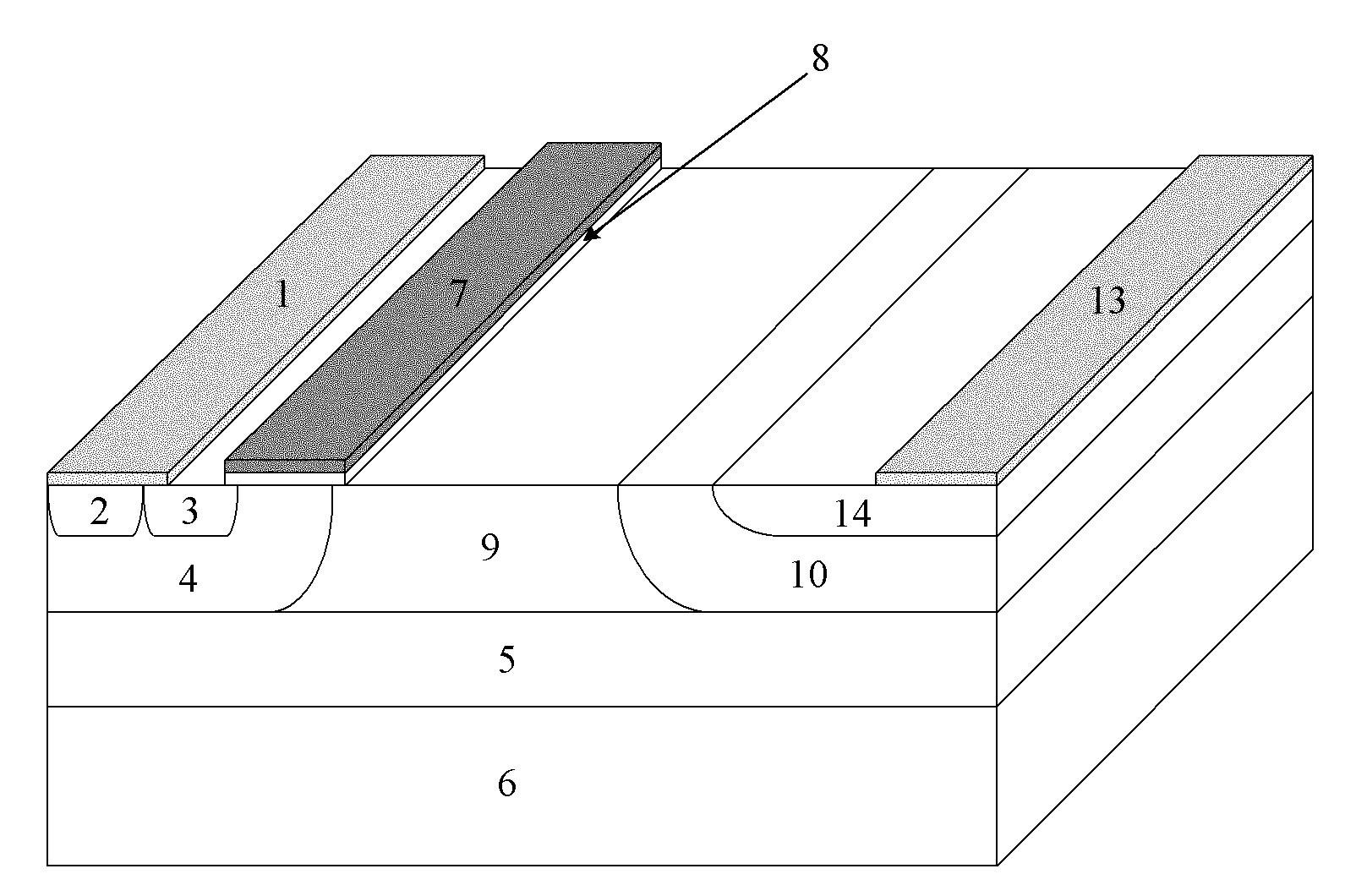
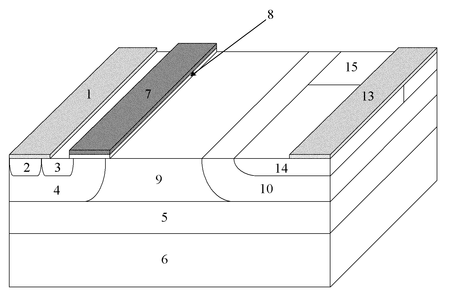
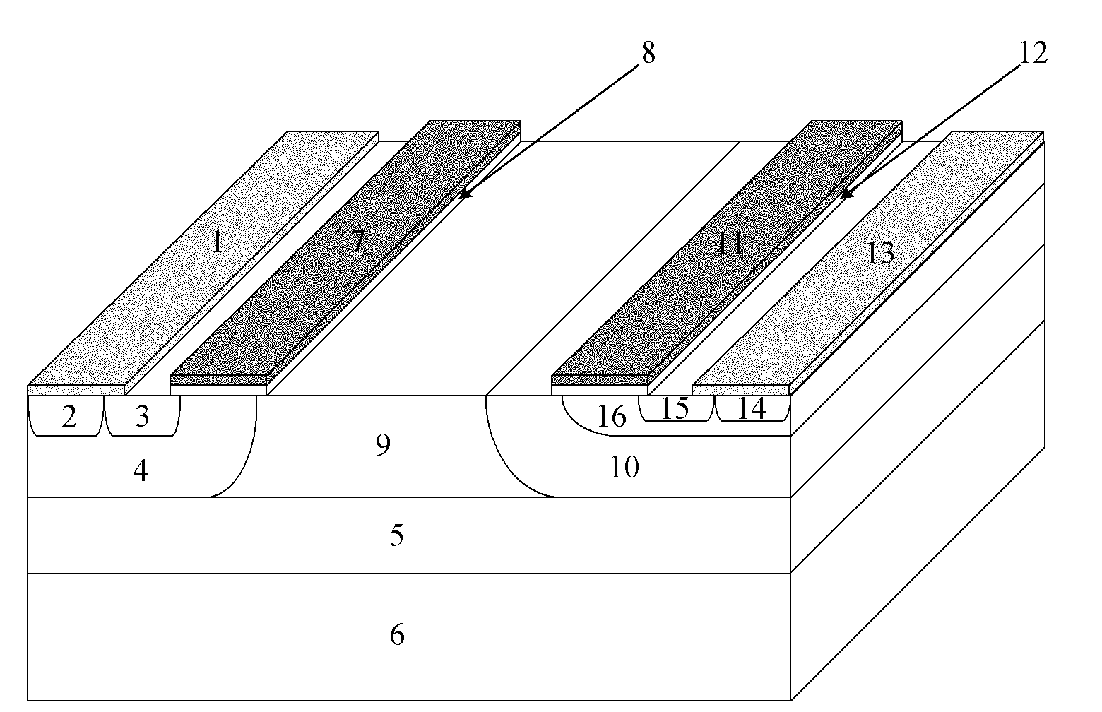
[0019] like Figure 4 As shown, a SOI-LIGBT device with a split anode structure includes an N-type or P-type substrate 6, a buried oxide layer 5 on the surface of the N-type or P-type substrate 6, and a device layer on the surface of the buried oxide layer 5 , the device layer includes an intermediate N - Base area 9, located in N -The cathode region on one side of the base region 9 is located in the N - An anode region on the other side of the base region 9 and a gate region on the cathode region. The cathode region consists of a metallized cathode 1, a P-type body region 4, a P + Cathode 2 and N + The cathode 3 is composed of the P-type body region 4 located on the surface of the buried oxide layer 5 and connected with N - Base 9 contacts, P + Cathode 2 and N + The cathodes 3 are located side by side in the lateral direction in the P-type body region 4 and are con...


PUM


Abstract

The invention discloses an SOI-LIGBT (silicon on insulator-lateral insulated gate bipolar transistor) device with a split anode structure, belonging to the technical field of semiconductor power devices. The SOI-LIBGT device comprises a substrate layer, a buried oxide layer, an N-base region, a cathode region, an anode region and a gate region, wherein the cathode region and the anode region area are positioned on the two sides of the N-base region; and the gate region is positioned on the cathode region. The anode region is split into a first anode region and a second anode region by an isolation groove, but the first anode region and the second anode region are still kept in electric connection. The first anode region ensures high hole injection efficiency when the device works; and the second anode region has a function of eliminating the negative differential resistance (NDR) area when the device is opened and provides an electron extraction channel at the turn-off transient state of the device. Through the invention, the NDR area introduced into positive characteristics in the anode short-circuit structure is eliminated on one hand, and on the other hand, the on resistance is increased while the turn-off speed is increased, and a good eclectic relationship between the conduction loss and the turn-off loss is obtained; and moreover, the manufacturing process of the device is compatible with a conventional power integrated circuit process, and additional steps or cost is not increased.

Description

technical field [0001] The invention belongs to the technical field of semiconductor power devices, and relates to conductance modulation high-voltage power devices, in particular to a SOI-LIGBT device (SOI: Silicon On Insulator, silicon on insulating layer; LIGBT: Lateral Insulated Gate Bipolar Transistor, insulated gate bipolar transistor ). Background technique [0002] SOI-LIGBT device is a key component of SOI high-voltage integrated circuits. It has the advantages of large current capacity and easy integration, but its switching speed is much faster than that of lateral double-diffused metal-oxide-semiconductor effect transistor (LDMOS, LateralDouble-diffused MOSFET. ) has a slow turn-off speed, resulting in a large switching loss, which affects the application of SOI lateral insulated gate bipolar transistors in power integrated circuits. [0003] The structure of a conventional SOI-LIGBT device is as figure 1 As shown, it includes: substrate layer 6, buried oxide l...

Claims


Application Information

Patent Timeline
IPC IPC(8): H01L29/739H01L29/08H01L29/417
Inventor 张波陈文锁乔明方健李肇基
Owner UNIV OF ELECTRONICS SCI & TECH OF CHINA
Why Eureka
Try Eureka