Structure and method for measuring electric property change of MOSFET (metal-oxide-semiconductor field effect transistor) device

A technology of electrical characteristics and measurement methods, applied in the direction of semiconductor/solid-state device testing/measurement, single semiconductor device testing, etc., can solve the problem that the change of polysilicon line width and the change of MOSFET electrical characteristics cannot be obtained, and the change and increase of polysilicon line width cannot be obtained. difficulty, etc.

Active Publication Date: 2011-08-17
SHANGHAI INTEGRATED CIRCUIT RES & DEV CENT
View PDF5 Cites 13 Cited by
  • Summary
  • Abstract
  • Description
  • Claims
  • Application Information

AI Technical Summary

Problems solved by technology

The traditional method is to optically measure the polysilicon line width online, which requires measurement at a specific time, that is, after a specific process step. Offline measurement cannot be performed. Once a specific process step is missed, the polysilicon line width cannot be measured. If a piece of If the wafer is not measured in the factory, the device engineer will not be able to know the change of the polysilicon line width, which requires the cooperation of the process, measurement and device departments, which increases the difficulty of implementation
Moreover, the traditional method of polysilicon line width measurement and MOSFET electrical measurement is separated, each has its own test structure, and the one-to-one correspondence between polysilicon line width changes and MOSFET electrical characteristics changes cannot be obtained.

Method used


Image

  • Structure and method for measuring electric property change of MOSFET (metal-oxide-semiconductor field effect transistor) device
  • Structure and method for measuring electric property change of MOSFET (metal-oxide-semiconductor field effect transistor) device

Examples


Embodiment Construction

[0015] In order to make the above objects, features and advantages of the present invention more obvious and comprehensible, specific implementations of the present invention will be described in detail below.

[0016] The measurement structure and measurement method for the electrical characteristic change of the MOSFET device described in the present invention can be realized by various replacement methods, and the following is illustrated by a preferred embodiment. Of course, the present invention is not limited to this specific embodiment. Common substitutions known to those of ordinary skill in the art undoubtedly fall within the protection scope of the present invention.

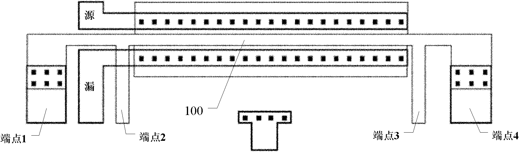
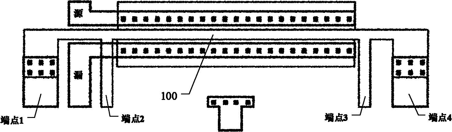
[0017] Please see figure 1 , figure 1 It is a structural schematic diagram of the measurement structure of the electrical characteristic change of the MOSFET device of the present invention. like figure 1 As shown, the MOSFET device electrical characteristic change measurement structure of the prese...


PUM


Abstract

The invention provides a structure for measuring electric property change of MOSFET (metal-oxide-semiconductor field effect transistor) device, which comprises an active area, a grid electrode located on the active area, wherein the grid electrode is a resistor in Kelvin structure; two ends of the grid electrode have two polyresistor end points. The structure of the invention has the advantage that the influences of the grid length change, the gate oxide thickness change and the doping change to the MOSFET device are distinguished and determined; and the three process changes are the main factors of electrical fluctuations of device and are the primary parameters for building a monte carlo model and a corner mode of the device; the determination of the three process changes can lead the monte carlo model and the corner model to be more precise, which is quite important under the condition that the requirements on process corner models that is more than 90nm are higher and higher, and in favour of extracting a stress model of the device for placing numbers and distances of different virtual grid electrodes in more than 45nm of process. The invention further provides a method for measuring electric property change of MOSFET device.

Description

technical field [0001] The invention relates to the technical field of semiconductor manufacturing, in particular to a measurement structure and a measurement method for the electrical characteristic change of a MOSFET device. Background technique [0002] In the process of 90nm or more, due to the small feature size, the gate length variation of MOSFETs at different positions in the wafer has a very obvious impact on the turn-on current. The gate length variation is divided into the variation of different positions inside the chip (local variation: local variation) and the variation between different chips (global variation: global variation). Determining the gate length variation can more accurately establish the Monte Carlo (monte carlo) model and corner (corner) model of the device. The traditional method is to optically measure the polysilicon line width online, which requires measurement at a specific time, that is, after a specific process step. Offline measurement c...

Claims


Application Information

Patent Timeline
Patent Type & Authority Applications(China)
IPC IPC(8): H01L21/66G01R31/26
Inventor 彭兴伟胡少坚任铮
Owner SHANGHAI INTEGRATED CIRCUIT RES & DEV CENT
Why Eureka
Try Eureka