Clock frequency multiplier, device and clock frequency multiplication method

A technology of clock frequency multiplication and frequency multiplication, which is applied in pulse processing, electrical components, pulse technology, etc., and can solve problems such as error-prone, clock output signal cycle changes, and logic errors.

Active Publication Date: 2011-08-17
LOONGSON TECH CORP
View PDF8 Cites 26 Cited by
  • Summary
  • Abstract
  • Description
  • Claims
  • Application Information

AI Technical Summary

Problems solved by technology

However, the design of the PLL structure is too complicated and the stability is poor, and the anti-radiation performance of the entire PLL loop is poor, and errors are prone to occur under radiation exposure conditions.
[0003] Moreover, most of the existing...

Method used


Image

  • Clock frequency multiplier, device and clock frequency multiplication method
  • Clock frequency multiplier, device and clock frequency multiplication method
  • Clock frequency multiplier, device and clock frequency multiplication method

Examples


Embodiment 1

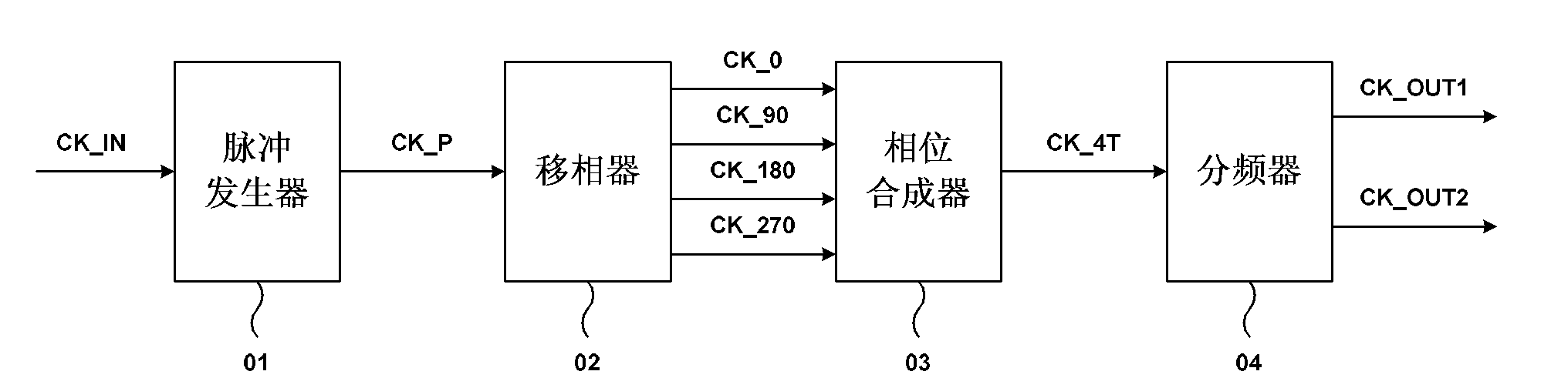
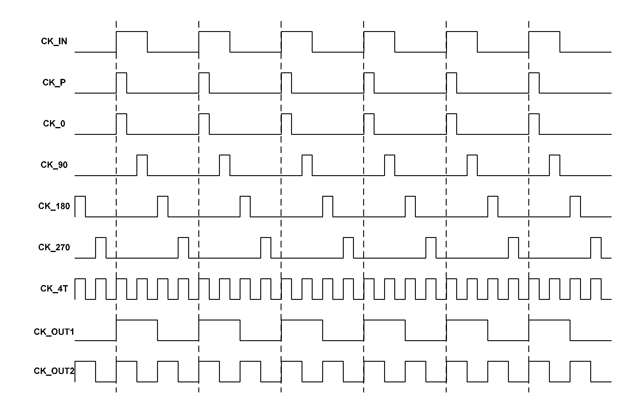
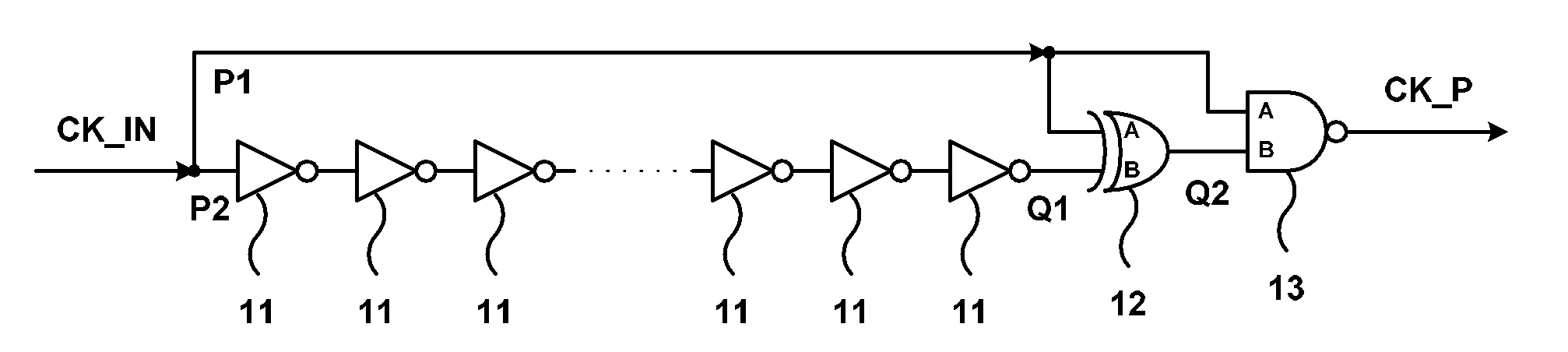
[0100] Embodiment 1: A clock frequency interrogator

[0101] As a preferred implementable mode, since the storage unit and calculation unit of some microprocessors use different clock domains, an on-chip clock source including a clock multiplier is required to generate clocks with good duty cycles at different frequencies Signal. Therefore, in the embodiment of the present invention, the clock frequency multiplier and device and the clock frequency multiplication method of the embodiment of the present invention are applied to the Loongson No. 1 microprocessor, and the external crystal oscillator signal provides the circuit with a clock signal with a frequency of 50-100 MHz , and the duty cycle is not ideal at 50%. After frequency multiplication processing, a double frequency clock signal is generated as an example for detailed description.

[0102] However, it should be noted that the clock frequency multiplier and device and clock frequency multiplication method of the pres...

Embodiment 2

[0187] Embodiment 2: An improved clock period measurement unit

[0188] In the embodiment of the present invention, the D-type flip-flop can be implemented by using a D-type transistor as a sampling tool, and its output result is a number of continuous 1 signals followed by a number of continuous 0 signals. The signal becomes a 1 signal, as long as it is not at the junction of the 1 signal and the 0 signal, it has no effect on the circuit. However, if the latch state of the 1 signal changes from a 1 signal to a 0 signal, the delay in the digitally controlled delay 23 will be changed, thereby causing an error.

[0189] Therefore, in the embodiment of the present invention, as another possible implementation mode, the embodiment of the present invention provides a clock period measurement unit, such as Figure 13 shown.

[0190] As another possible implementation, a clock period measurement unit in the embodiment of the present invention includes four two-input NAND logic gate...

Embodiment 3

[0193] Embodiment 3: An improved two-input NAND logic gate circuit device, and an improved non-logic gate circuit device

[0194] When the threshold voltage of the N-type field effect transistor drifts downward, the N-type field effect transistor in the logic gate circuit will be easily turned on, thereby changing the working state of the circuit. Therefore, in the embodiment of the present invention, as another possible Embodiments provide a two-input NAND logic gate circuit device, such as Figure 15 shown; and a non-logic gate circuit device, such as Figure 14 shown.

[0195] In the embodiment of the present invention, as another possible implementation mode, such as Figure 14 As shown, the non-logic gate circuit device 16 of the embodiment of the present invention is composed of two N-type field effect transistors and two P-type field effect transistors.

[0196] The N-type field effect transistor substrate is connected to VSS, the P-type field effect transistor subst...


PUM


Abstract

The invention discloses a clock frequency multiplier, a clock frequency multiplication device and a clock frequency multiplication method. The clock frequency multiplier comprises a pulse generator, a phase shifter, a phase synthesizer and a frequency divider, wherein the pulse generator is used for regulating an external input clock signal into an equal periodic pulse clock signal; the phase shifter is used for performing phase shifting on the input equal periodic pulse clock signal for different time lengths according to a required frequency multiplication fold and a clock cycle to obtain phase shifted clock signals; the phase synthesizer is used for performing phase synthesis on the equal periodic pulse clock signal and each phase shifted clock signal to obtain a frequency multiplied clock signals; and the frequency divider is used for performing frequency division on the phase-synthesized frequency multiplied clock signal to obtain a frequency multiplied output clock signal, and outputting the frequency multiplied output clock signal. By the clock frequency multiplier, the clock frequency multiplication device and the clock frequency multiplication method, the frequency multiplication of the clock signal is realized under the condition of no phase-locked loops, and/or normal operations can be realized under the condition of radiation exposure.

Description

technical field [0001] The invention belongs to integrated circuits of frequency synthesizers, in particular to a clock multiplier and device and a clock frequency multiplication method, more specifically to a clock multiplier and device and a clock for anti-irradiation integrated circuits Doubling method. Background technique [0002] At present, clock frequency multipliers are widely used in integrated circuits. In the prior art, a phase-locked loop (PLL) is generally used as a clock frequency multiplier to increase the frequency of an input clock signal. However, the structural design of the phase-locked loop is too complicated and the stability is poor, and the anti-irradiation performance of the entire phase-locked loop loop is poor, and errors are prone to occur under radiation exposure conditions. [0003] Moreover, most of the existing frequency multiplication technologies use counters or shift registers as the state memory. When this state memory encounters radiati...

Claims


Application Information

Patent Timeline
IPC IPC(8): H03K5/00
Inventor 于航杨旭
Owner LOONGSON TECH CORP
Why Eureka
Try Eureka