
Manufacturing method of EDMOS (Extended Drain Metal Oxide Semiconductor) device

A manufacturing method and device technology, applied in the fields of semiconductor/solid-state device manufacturing, electrical components, circuits, etc., can solve the problems affecting the yield rate of EDMOS devices, operation errors, and complex layout, and achieve simplified layout, simple isolation, and improved yield. Effect

Inactive Publication Date: 2011-09-14
SHANGHAI HUAHONG GRACE SEMICON MFG CORP
View PDF6 Cites 2 Cited by
  • Summary
  • Abstract
  • Description
  • Claims
  • Application Information

AI Technical Summary

Problems solved by technology

[0005] In practice, it has been found that in the prior art method of manufacturing EDMOS devices, the layout is complicated during the deposition of the silicide barrier layer and the source / drain ion implantation barrier layer, and it is difficult to implement the self-alignment process, and there are operational errors in actual operation. When the distance from the drain to the gate is less than 2um, especially when the distance from the drain to the gate is less than 1um, this error will dominate and seriously affect the yield of the manufactured EDMOS devices

Method used


Image

  • Manufacturing method of EDMOS (Extended Drain Metal Oxide Semiconductor) device
  • Manufacturing method of EDMOS (Extended Drain Metal Oxide Semiconductor) device
  • Manufacturing method of EDMOS (Extended Drain Metal Oxide Semiconductor) device

Examples


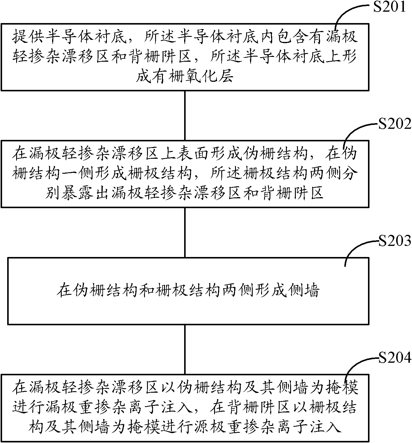
Embodiment Construction

[0035] In order to make the above-mentioned objects, features and advantages of the present invention more obvious and understandable, the specific embodiments of the present invention will be described in detail below with reference to the accompanying drawings.

[0036] In the following description, many specific details are set forth in order to fully understand the present invention, but the present invention can also be implemented in other ways different from those described herein, so the present invention is not limited by the specific embodiments disclosed below.

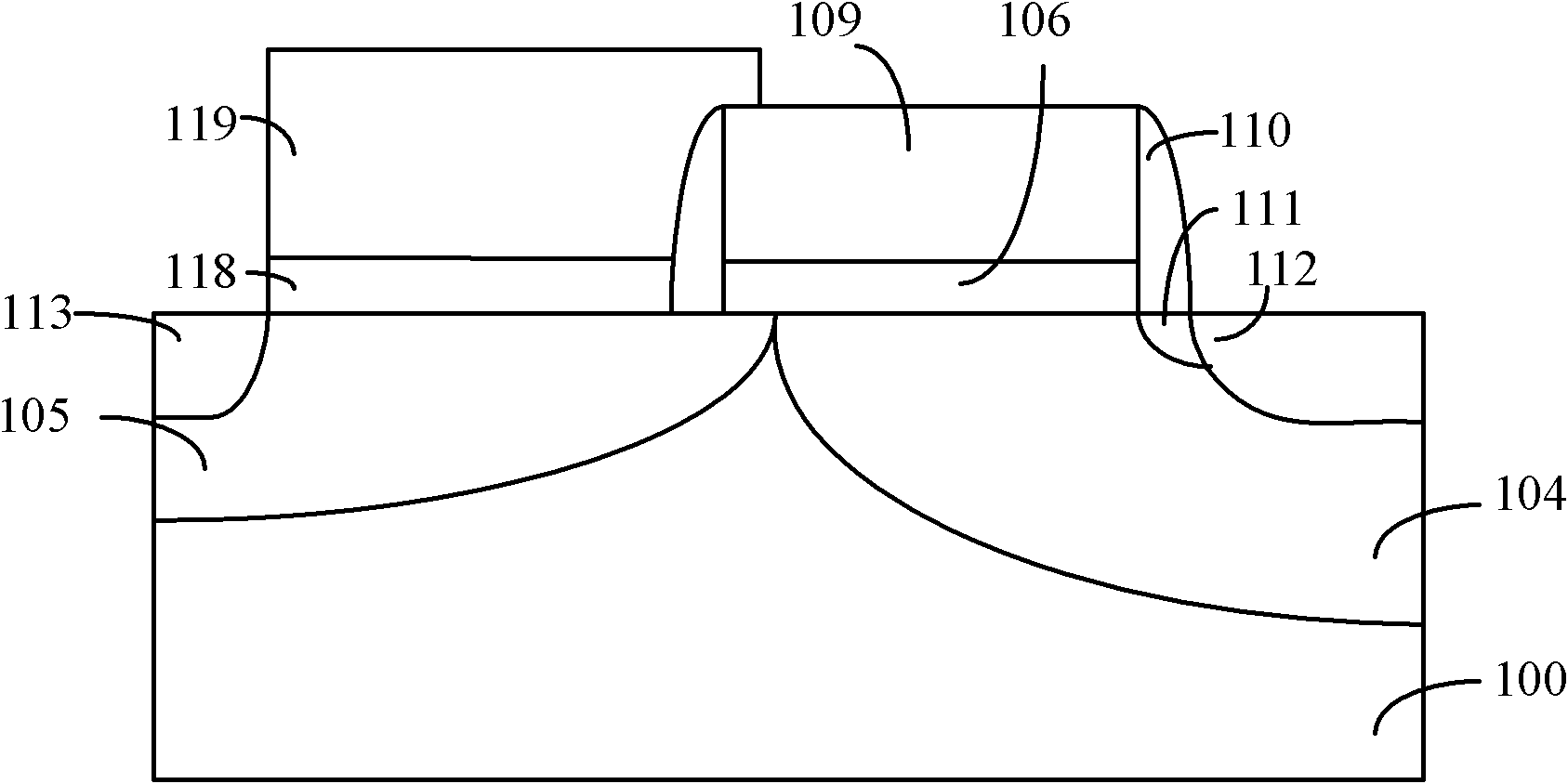
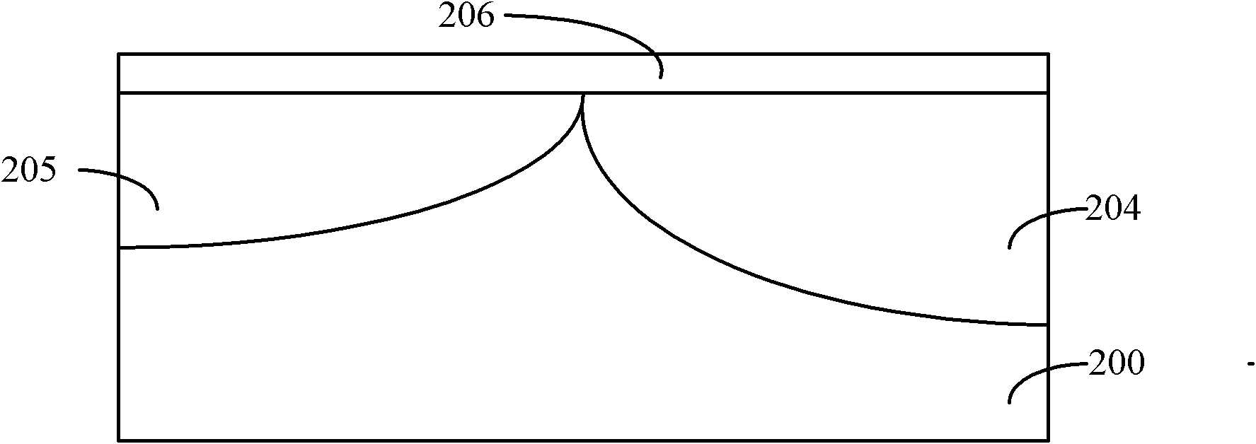
[0037] As mentioned in the background art section, the prior art mainly increases the channel width by sequentially depositing a silicide barrier layer and a source / drain ion implantation barrier layer on the semiconductor substrate on the drain extension region of the DEMOS device. The layout is complex and there are operational errors in the process of implementation. When the distance from the drain to the gat...


PUM

PropertyMeasurementUnit
Width rangeaaaaaaaaaa
Widthaaaaaaaaaa

Abstract

The invention relates to a manufacturing method of an EDMOS (Extended Drain Metal Oxide Semiconductor) device, wherein a process of depositing a pseudo grid structure on a semiconductor substrate above an EDMOS device drain extension area takes the place of a traditional process of depositing a salicide block (SAB) layer and a source / drain ion implant block layer, thus a breakdown voltage of the EDMOS device is increased. By utilizing the manufacturing method of the EDMOS, EDMOD devices sharing the drain can be further manufactured and have the advantages that the isolation among the devices becomes simpler and the structure extension is convenient. According to the manufacturing method of the EDMOS disclosed by the invention, the layout is simple; the operating errors generated in the manufacturing process of the EDMOS device, in which the distance between the drain and the grid is smaller than 2 microns, due to depositing of the SAB layer and source / drain ion implant block layer are effectively reduced; and the yield of the manufactured EDMOS devices is increased.

Description

Technical field [0001] The present invention relates to the field of semiconductor technology, and more specifically, the present invention relates to a manufacturing method of an Extended Drain Metal Oxide Semiconductor (EDMOS) device. Background technique [0002] MOS high-voltage devices have a wide range of applications in chips such as LCD panel drive, power management, and DC / AC converters. Evaluating the performance of high-voltage devices generally includes three indicators: breakdown voltage, on-resistance, and switching speed; evaluating the reliability of high-voltage devices generally includes two indicators: safe working area and performance degradation caused by hot electron injection. [0003] The type of MOS device used in semiconductor devices is an N or P-channel drain extended metal oxide semiconductor (EDMOS) device, which utilizes a drain extension region to increase the operating voltage of the device, and is usually used in, for example, power conversion circ...

Claims


Application Information

Patent Timeline
IPC IPC(8): H01L21/336H01L21/8234
Inventor 刘正超
Owner SHANGHAI HUAHONG GRACE SEMICON MFG CORP
Features
  • Generate Ideas
  • Intellectual Property
  • Life Sciences
  • Materials
  • Tech Scout
  • Unparalleled Data Quality
  • Higher Quality Content
  • 60% Fewer Hallucinations
Learn More