Junction terminal structure of lateral power device

A lateral power device and junction terminal technology, applied in semiconductor devices, electrical components, circuits, etc., can solve the problems of difficult adjustment, complex preparation process, complex voltage divider network, etc., and achieve improved breakdown voltage and drift region concentration. Value improvement, good I-V characteristics

Inactive Publication Date: 2011-09-14
NANJING UNIV OF POSTS & TELECOMM
View PDF10 Cites 17 Cited by
  • Summary
  • Abstract
  • Description
  • Claims
  • Application Information

AI Technical Summary

Problems solved by technology

However, for lateral power devices with this structure, the voltage divider network is more complicated and not easy to adjust
[0007] The various structures mentioned above all prepare field plates on the surface of power devices to adjust the surface electric field, but the preparation process of multi-step and inclined field plates on the surface is very complicated, and the effect is not very ideal

Method used


Image

  • Junction terminal structure of lateral power device
  • Junction terminal structure of lateral power device
  • Junction terminal structure of lateral power device

Examples


Embodiment Construction

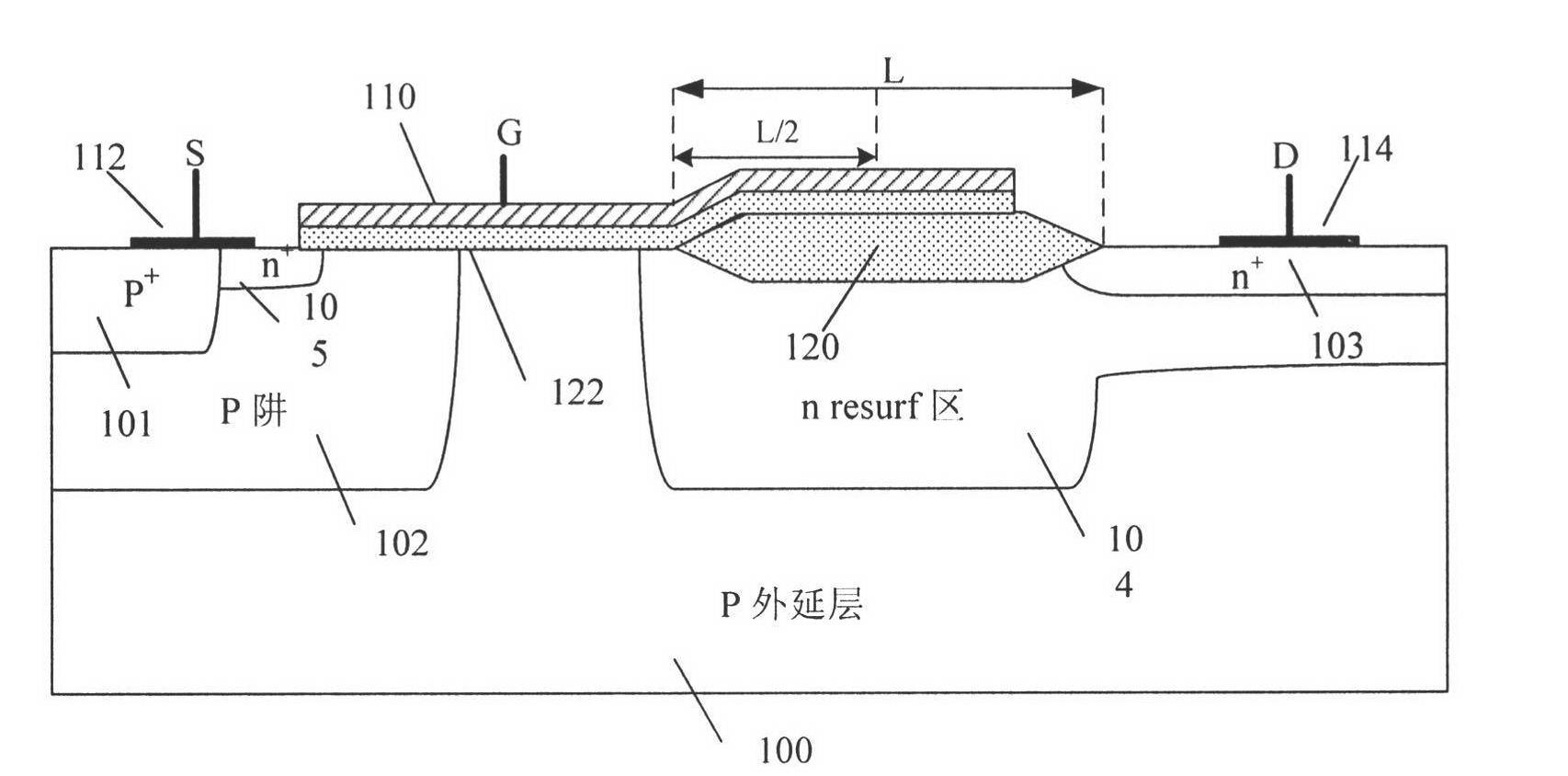
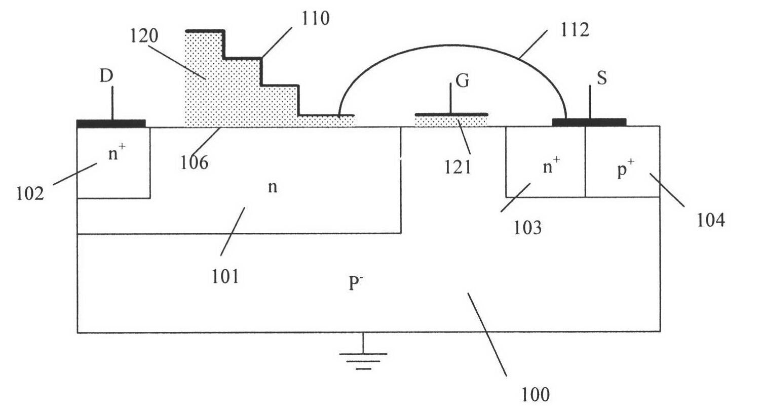
[0038] The invention provides a junction termination structure in a lateral power device. Figure 5 is the 3D view of the structure, Figure 6 a is the top view of the structure, Figure 6 b is the structure along Figure 6 Sectional view of line AB in a, Figure 6 c is the structure along the Figure 6 Cross-sectional view of the CD line in a. It can be seen that in the silicon base on the substrate region 100 of the first conductivity type, the semiconductor region 101 of the first conductivity type with a high doping concentration is formed by twice high doping, and the high doping concentration The semiconductor region 103 of the second conductivity type, the two are connected by the semiconductor region 102 of the second conductivity type with a light doping concentration, the semiconductor region 102 is used as a drift region, and the sidewall of the semiconductor region 102 is filled with field oxygen to form a connection with it The sidewall oxide layer 120 is jux...


PUM


Abstract

The invention discloses a junction terminal structure of a lateral power device. The structure at least comprises three semiconductor doping regions, a side wall oxidation zone and a side wall field plate region, which are sequentially connected, wherein the side wall field plate region is positioned at the two ends of the device; the doping region positioned at one end is a first kind of conducting type and forms a channel region (or the anode) of the device; the doping region positioned at the other end is a second kind of conducting type and forms a drain electrode region (or the cathode) of the device; the semiconductor doping region positioned in the middle is the second kind of conducting type and forms a drift region of the device; the lower part of the drift region is connected with an epitaxial layer; the upper part of the drift region is connected with a field oxide layer; the side of the drift region is connected with an oxidation zone; polysilicon is etched and deposited in the side wall oxidation zones of a source area and a drain area to form a slope-shaped or multi-step shaped three-dimensional (3D) field plate; the field plate is in electric contact with a grid electrode and a drain electrode respectively; and the side wall field plate is required to extend into the surface of a substrate to enter the substrate. When a PN diode, a lateral diffused metal oxide semiconductor (LDMOS) or a lateral insulated gate bipolar transistor (LIGBT) is manufactured through the structure, the structure has the advantages of high breakdown voltage, low on resistance, simpleprocess, low cost and the like.

Description

technical field [0001] The invention belongs to the field of semiconductor power device technology and semiconductor technology, and particularly relates to the junction terminal technology of lateral power devices for high-power and high-voltage applications, such as lateral diffusion field effect transistor LDMOS, lateral high-voltage diode, lateral insulated gate bipolar transistor LIGBT and the like. Background technique [0002] As we all know, in the design process of lateral power devices, the interaction of factors such as breakdown voltage, on-resistance, process complexity, and reliability must be considered comprehensively to achieve a reasonable compromise. Usually, the improvement of one aspect of performance often leads to the degradation of other aspects of performance, and there is such a contradictory relationship between breakdown voltage and on-resistance. How to keep the on-resistance constant or minimize the on-resistance while increasing the breakdown v...

Claims


Application Information

Patent Timeline
Patent Type & Authority Applications(China)
IPC IPC(8): H01L29/40H01L29/78H01L29/739
CPCH01L29/7835H01L29/0653H01L29/402H01L29/404H01L29/407H01L29/42368H01L29/7816
Inventor 郭宇锋钟大伟夏晓娟张长春张瑛
Owner NANJING UNIV OF POSTS & TELECOMM
Why Eureka
Try Eureka