An etching method for HgCdTe material with low damage and high uniformity

A mercury cadmium telluride, low-damage technology, applied in the direction of climate sustainability, sustainable manufacturing/processing, electrical components, etc., can solve the problems of surface atom chemical ratio imbalance, lower device performance, material type inversion, etc., to achieve Good I-V characteristics, excellent chip performance, and low damage effects

Active Publication Date: 2016-04-27
11TH RES INST OF CHINA ELECTRONICS TECH GROUP CORP
View PDF3 Cites 0 Cited by
  • Summary
  • Abstract
  • Description
  • Claims
  • Application Information

AI Technical Summary

Problems solved by technology

The mercury cadmium telluride material used to prepare the chip is fragile due to its own chemical bond, and it is easy to break when it receives the action of external ions, resulting in an imbalance in the chemical ratio of the surface atoms, and in severe cases, the material type is reversed. Introducing a pn junction, which degrades device performance

Method used


Image

  • An etching method for HgCdTe material with low damage and high uniformity
  • An etching method for HgCdTe material with low damage and high uniformity
  • An etching method for HgCdTe material with low damage and high uniformity

Examples


Embodiment 1

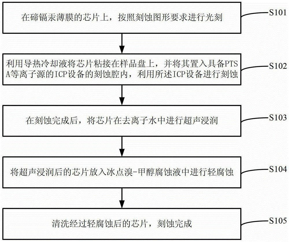
[0024] An embodiment of the present invention provides an etching method for HgCdTe material with low damage and high uniformity, such as figure 1 shown, including the following steps:

[0025] Step S101, performing photolithography on the HgCdTe thin film chip according to the etching pattern requirements;

[0026] Step S102, using heat conduction cooling liquid to bond the chip on the sample tray, and placing it into the etching chamber of the ICP equipment equipped with a PTSA plasma source, and using the ICP equipment to perform etching;

[0027] Step S103, after the etching is completed, ultrasonically infiltrate the chip in deionized water;

[0028] Preferably, in this step, the ultrasonic frequency used for ultrasonic infiltration is 20kHz-80kHz, and the power is 50W-150W.

[0029] Preferably, in this step, the time for ultrasonic infiltration is 3 minutes to 6 minutes.

[0030] Step S104, putting the ultrasonically wetted chip into a freezing point bromine-methanol ...

Embodiment 2

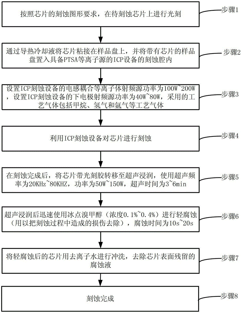
[0036] An embodiment of the present invention provides an etching method for HgCdTe material with low damage and high uniformity. The basic principle of this embodiment is the same as that of Embodiment 1, and it is a further detailed elaboration of the method described in Embodiment 1 in conjunction with the accompanying drawings. .

[0037] The method described in the embodiment of the present invention mainly incorporates the following technologies:

[0038] (1) Chip etching is performed using ICP (Inductively Coupled Plasma Etching) etching equipment using a PTSA (Plant Triple Helix Antenna) type ion source. Among them, the PTSA-type ion source has the ability to provide more efficient RF coupling and generate higher-density plasma under the condition of low RF power. The uniformity of etching is reduced due to temperature inhomogeneity; at the same time, the plasma generated by the PTSA ion source has lower energy (<20eV), which can better reduce the damage in the etchin...


PUM


Abstract

The invention discloses a low-damage high-uniformity etching method for hgcdte materials. The etching method includes steps of 1), photoetching according to an etching graphic on a chip of a hgcdte film; 2), adhering the chip to a sample disc by heat conduction cooling liquid prior to placing the chip in an etching chamber of an ICP (inductively coupled plasma) device with PTSA (panel three spiral antenna) plasma source, and etching by utilizing the ICP device; 3), subjecting the etched chip to ultrasonic infiltration in deionized water after etching; 4), placing the chip into bromine-methanol corrosive liquid for mild etching after the ultrasonic infiltration; and 5) cleaning the etched chip to finish the etching. Based on an ICP etching with the PTSA plasma source, combined with a mild etching process of the ultrasonic infiltration with bromine methanol at freezing point and assisted with special high heat conduction adhesives, the etching method can remove affected layers of the hgcdte materials which appear easily during the etching process, so that a low-damage high-uniformity etching effect is realized.

Description

technical field [0001] The invention relates to the technical field of semiconductors, in particular to an etching method for HgCdTe materials with low damage and high uniformity. Background technique [0002] Infrared focal plane detection technology has significant advantages such as wide spectral response band, more ground target information can be obtained, and can work day and night. It is widely used in early warning detection, intelligence reconnaissance, damage effect assessment, and investigation, development and Management, weather forecast, geothermal distribution, earthquake, volcanic activity, space astronomical exploration and other fields. [0003] HgCdTe infrared detector chip is one of the representative products of infrared detection technology. There are many processes to prepare this chip, including semiconductor device processes such as photolithography, ion implantation, passivation, electrode deposition, and etching. Among them, etching is the main m...

Claims


Application Information

Patent Timeline
Patent Type & Authority Patents(China)
IPC IPC(8): H01L31/18
CPCY02P70/50
Inventor 谭振陈慧卿史春伟李龙
Owner 11TH RES INST OF CHINA ELECTRONICS TECH GROUP CORP
Why Eureka
Try Eureka