SIC ohmic contact structure and manufacturing method thereof

A manufacturing method, ohmic contact technology, applied in semiconductor/solid-state device manufacturing, semiconductor devices, electrical components, etc., can solve the problems of reduced reliability of ohmic contact electrodes, limited application environment and scope, mechanical damage, etc., and achieve good I-V characteristics , Improve the effect of thermal stability and oxidation resistance

Active Publication Date: 2020-02-07
XIDIAN UNIV
View PDF3 Cites 0 Cited by
  • Summary
  • Abstract
  • Description
  • Claims
  • Application Information

AI Technical Summary

Problems solved by technology

[0004] At present, the problems faced by silicon carbide ohmic contact metal or alloy layer include weak oxidation resistance, which is oxidized in the air; poor thermal stability, degradation or failure at high temperature; low hardness, easy to be mechanically damaged, etc. These shortcomings will make The reliability of ohmic contact electrodes is reduced, which severely limits its application environment and scope, which in turn affects and limits the application scope and reliability of silicon carbide devices

Method used


Image

  • SIC ohmic contact structure and manufacturing method thereof
  • SIC ohmic contact structure and manufacturing method thereof
  • SIC ohmic contact structure and manufacturing method thereof

Examples


Embodiment 1

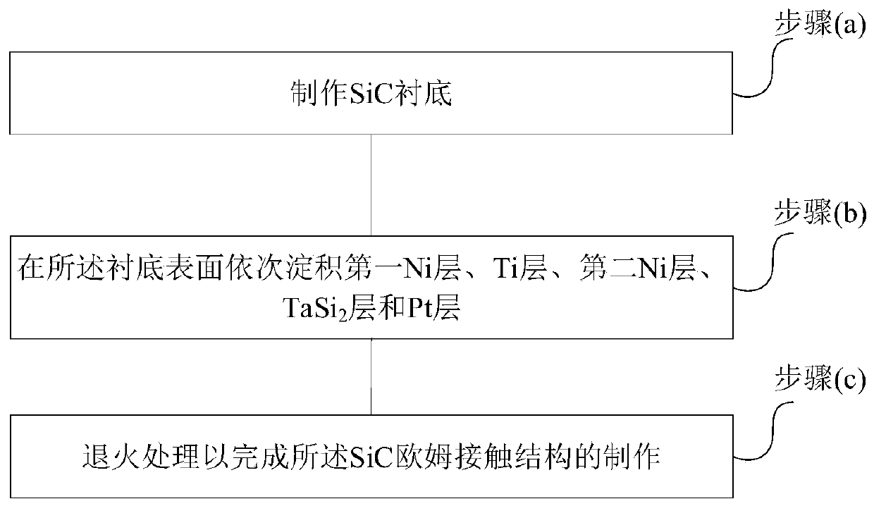
[0040] See figure 1 , figure 1 A SiC ohmic contact process flow chart provided for an embodiment of the present invention, including:

[0041] (a) making a SiC substrate;

[0042] (b) sequentially depositing a first Ni layer, a Ti layer, a second Ni layer, TaSi on the substrate surface 2 layer and Pt layer;

[0043] (c) performing a first annealing treatment to complete the fabrication of the SiC ohmic contact structure.

[0044] Preferably, step (a) may include:

[0045] (a1) selecting a 4H-SiC substrate and performing standard RCA cleaning on the 4H-SiC substrate;

[0046] (a2) Depositing an oxide layer with a thickness of 100 nm on the surface of the 4H-SiC substrate by PECVD process;

[0047] (a3) Etching the oxide layer to form an ion implantation window, and performing N on the surface of the 4H-SiC substrate by using an ion implantation process + ,P + Ion implantation forms N-type doped regions and P-type doped regions;

[0048] (a4) Etching away the remaining ...

Embodiment 2

[0065] The present invention proposes a kind of utilization Pt / TaSi 2 / Ni / Ti / Ni / SiC structure method for making SiC ohmic contacts, including:

[0066] S201, select a 4H-SiC substrate, and perform standard RCA cleaning on the 4H-SiC substrate;

[0067] S202, using the PECVD process, deposit SiO with a thickness of 100nm on the 4H-SiC substrate 2 oxide layer;

[0068] S203, etching the oxide layer to form an ion implantation window, for 4H-SiC substrate N + or P + Ion implantation to form highly doped N or P regions and perform high temperature annealing;

[0069] S204, etching the remaining oxide layer;

[0070] S205, depositing a metal layer on the 4H-SiC substrate, the metal layer sequentially includes a first Ni layer, a Ti layer, a second Ni layer, TaSi 2 layer and Pt layer;

[0071] S206 , rapid annealing to form an ohmic contact.

[0072] Preferably, the doping source of the N-type doping region in step S203 is Al, and the doping concentration is 1.0×10 20 cm -...

Embodiment 3

[0090] Please refer to Figure 9 , Figure 9 A cross-sectional view of a SiC ohmic contact structure provided for an embodiment of the present invention; the SiC ohmic contact structure includes: a SiC substrate 1, and a first Ni layer 2, a Ti layer 3, and a second Ni layer arranged on the SiC substrate in sequence. Ni layer 4, TaSi 2 Layer 5 and Pt layer 6.


PUM

PropertyMeasurementUnit
thicknessaaaaaaaaaa
thicknessaaaaaaaaaa
thicknessaaaaaaaaaa

Abstract

The invention relates to a SiC ohmic contact structure and a fabrication method thereof. The fabrication method comprises the steps of fabricating a SiC substrate; sequentially depositing a first Ni layer, a Ti layer, a second Ni layer, a TaSi2 layer and a Pt layer on a surface of the substrate; and performing annealing to complete fabrication of the SiC ohmic contact structure. With the SiC ohmiccontact proposed by the invention, the thermal stability and the oxidization resistant performance of the ohmic contact are improved.

Description

technical field [0001] The invention belongs to the field of silicon carbide device manufacturing, and in particular relates to a SiC ohmic contact structure and a manufacturing method thereof. Background technique [0002] Compared with traditional germanium and silicon materials, the advantages of the third-generation wide-bandgap semiconductor silicon carbide mainly include: the electric field withstand capacity is about ten times that of silicon materials, the band gap is about three times that of silicon materials, and the thermal conductivity is about 10 times that of silicon materials. Triple and so on. The above material characteristics make it show the incomparable advantages of traditional silicon-based devices under the conditions of extreme temperature (especially high temperature), high voltage, high frequency and high power, and strong radiation. [0003] Ohmic contact is one of the key factors affecting the application of silicon carbide devices in extreme en...

Claims


Application Information

Patent Timeline
Patent Type & Authority Patents(China)
IPC IPC(8): H01L21/04H01L29/45
Inventor 张艺蒙李彦良张玉明宋庆文汤晓燕
Owner XIDIAN UNIV
Why Eureka
Try Eureka