Manufacturing method for front electrode of crystalline silicon solar battery

A solar cell, front electrode technology, applied in circuits, electrical components, semiconductor devices, etc., can solve the problems of high sintering temperature, easy damage to silicon wafers, high price, etc., to reduce manufacturing costs, improve product quality, and reduce costs. Effect

Inactive Publication Date: 2011-09-14
NINGBO INST OF MATERIALS TECH & ENG CHINESE ACADEMY OF SCI
View PDF5 Cites 8 Cited by
  • Summary
  • Abstract
  • Description
  • Claims
  • Application Information

AI Technical Summary

Problems solved by technology

This technique has the following disadvantages: (1) silver is expensive as a noble metal, and the consumption of the front electrode material is very large, therefore, the cost of adopting this technique to prepare the front electrode of a crystalline silicon solar cell is very high; (2) in this technique, The sintering temperature is high, and there are problems such as easy damage to the silicon wafer, large product warpage, and high energy consumption.

Method used


Image

  • Manufacturing method for front electrode of crystalline silicon solar battery
  • Manufacturing method for front electrode of crystalline silicon solar battery

Examples


Embodiment 1

[0020] Step 1. Prepare indium gallium copper paste:

[0021] In a constant temperature operating table at 160°C, copper powder particles with a particle size of 2 microns to 20 microns and a purity of 99.99% are added to the indium gallium liquid alloy and stirred to form a viscous slurry. According to the mass percentage, in the entire mixture The content of copper powder is 60%;

[0022] Step 2. Preparation of selective emitter:

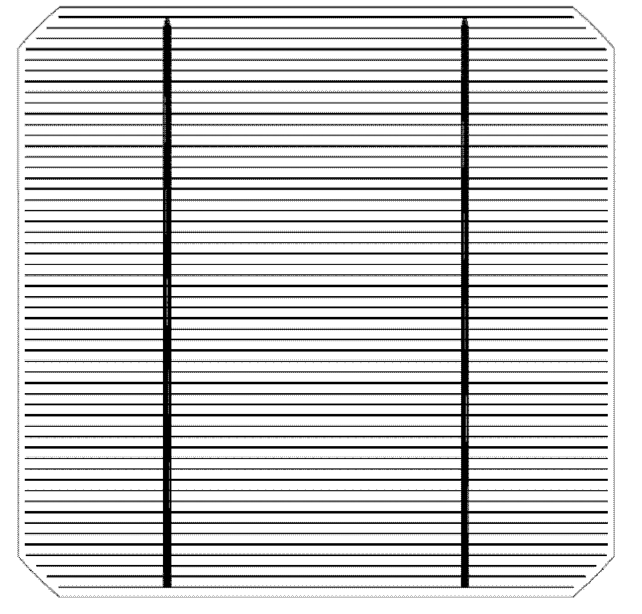
[0023] On the silicon wafer surface, press figure 1 The area shown is laser grooved on the silicon wafer to create a selective emitter;

[0024] Step 3. Screen printing front electrode:

[0025] Put the silicon wafer after the selective emitter preparation into the HF solution to remove the phosphosilicate glass layer, then take out the silicon wafer, and precisely print the composite paste on the figure 1 on the laser grooved area shown;

[0026] Step 3, low temperature sintering:

[0027] Put the silicon wafer into the sintering furnace and...

Embodiment 2

[0029] Step 1. Prepare indium gallium copper paste:

[0030] In a constant temperature operating table at 220°C, copper powder particles with a particle size of 2 microns to 20 microns and a purity of 99.99% are added to the indium gallium liquid alloy and stirred to form a viscous slurry. According to the mass percentage, in the entire mixture The content of copper powder is 80%;

[0031] Step 2. Preparation of selective emitter:

[0032] On the silicon wafer surface, press figure 1 The area shown is laser grooved on the silicon wafer to create a selective emitter;

[0033] Step 3. Screen printing front electrode:

[0034] Put the silicon wafer after the selective emitter preparation into the HF solution to remove the phosphosilicate glass layer, then take out the silicon wafer, and precisely print the composite paste on the figure 1 on the laser grooved area shown;

[0035] Step 3, low temperature sintering:

[0036] Put the silicon wafer into the sintering furnace and...


PUM

PropertyMeasurementUnit
Particle sizeaaaaaaaaaa

Abstract

The invention discloses a manufacturing method for a front electrode of a crystalline silicon solar battery, and the method comprises the following steps: on the basis of using a mixture of indium-gallium alloys with a low melting point and copper powder as a composite slurry, carrying out laser grooving on the front electrode region of a silicon slice so as to prepare a selective emitting electrode; then printing the composite slurry in the grooving region by utilizing a high-standard silk-screen printing process; and finally, carrying out the low-temperature sintering at 300-400 DEG C to form the front electrode. Compared with the prior art, the manufacturing method disclosed by the invention has the advantages that the manufacturing cost can be lowered, the sintering temperature is reduced, and the quality of a product is improved, thus the manufacturing method has important industrialization prospects in the field of crystalline silicon solar batterys.

Description

technical field [0001] The invention relates to the technical field of crystalline silicon solar cells, in particular to a method for manufacturing a front electrode of a crystalline silicon solar cell. Background technique [0002] A crystalline silicon solar cell is a semiconductor device that converts light energy directly into electrical energy. For the entire crystalline silicon solar cell device, the embodiment of the structure and performance needs to be realized through electrode sampling data. Therefore, in the manufacturing process of the crystalline silicon solar cell, after the PN junction is formed, the photoelectric current that can be collected can be derived. The front electrode is one of the key steps in the process, and the uniformity and conductivity of the front electrode have a great influence on the performance and yield of the product. [0003] The preparation methods of the front electrode of crystalline silicon solar cells can be divided into electr...

Claims


Application Information

Patent Timeline
IPC IPC(8): H01L31/18
CPCY02P70/50
Inventor 万青龚骏竺立强黄晋李莉
Owner NINGBO INST OF MATERIALS TECH & ENG CHINESE ACADEMY OF SCI
Why Eureka
Try Eureka