Preparation method of back contact HIT solar battery based on N-type silicon wafer
A solar cell, back-contact technology, applied in circuits, electrical components, final product manufacturing, etc., can solve the problems of high cost and small production capacity, achieve the effect of simple method, reduce component production cost, and avoid electrode shading
- Summary
- Abstract
- Description
- Claims
- Application Information
AI Technical Summary
Problems solved by technology
Method used
Image
Examples
Embodiment 1
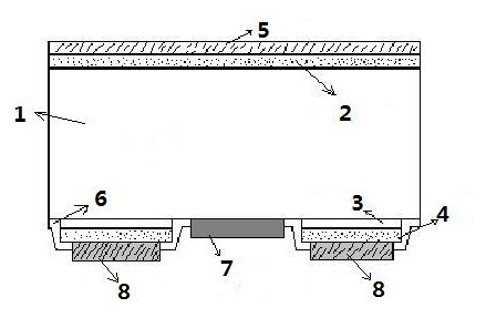
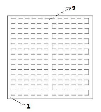
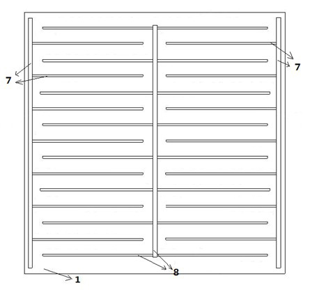
[0029] Select N-type monocrystalline silicon wafer; N-type silicon wafer 1 undergoes a conventional cleaning process, and the surface is subjected to alkali texturing to remove the mechanical damage layer on the surface of the silicon wafer, remove surface oil and metal impurities, and form a pyramid-shaped textured surface. Increase the absorption of sunlight, increase the area of the PN junction, and increase the short-circuit current. Use amorphous silicon coating equipment to deposit a layer of highly doped N+ type amorphous silicon thin layer 2 on the front surface of N-type silicon wafer 1, with a film thickness of 50nm, and then deposit a layer on the back surface of N-type silicon wafer 1 in sequence An intrinsic amorphous silicon thin layer 3 with a film thickness of 1 nm, and a P-type amorphous silicon thin layer 4 with a film thickness of 150 nm. On the screen printing machine, according to the attached drawings figure 2 The mask pattern shown in , on the back s...
Embodiment 2
[0031] Choose N-type polysilicon wafers; N-type silicon wafers 1 undergo conventional cleaning processes, and the surface is acid-textured in order to remove the mechanical damage layer on the surface of the silicon wafers, remove surface oil and metal impurities, and form undulating suede to increase sunlight resistance. The absorption increases the PN junction area and increases the short-circuit current. Use amorphous silicon coating equipment to deposit a layer of highly doped N+ type amorphous silicon thin layer 2 on the upper surface of N-type silicon wafer 1, the film thickness is 50nm, and then deposit a layer on the back surface of N-type silicon wafer 1 in sequence An intrinsic amorphous silicon thin layer 3 with a film thickness of 1 nm, and a p-type amorphous silicon thin layer 4 with a film thickness of 150 nm. On the screen printing machine, according to the attached drawings figure 2 The mask pattern shown in , on the back surface of the N-type silicon wafer 1...
PUM
| Property | Measurement | Unit |
|---|---|---|
| Thickness | aaaaa | aaaaa |
| Thickness | aaaaa | aaaaa |
| Thickness | aaaaa | aaaaa |
Abstract
Description
Claims
Application Information


