Substrate mould for microfluidic chip and manufacturing method thereof

A technology of a microfluidic chip and a manufacturing method, which is applied to the photoengraving process of the pattern surface, optics, optomechanical equipment and other directions, can solve problems such as pattern damage, and achieve the effect of preventing patterns

Inactive Publication Date: 2011-09-21
北京同方光盘股份有限公司
View PDF4 Cites 21 Cited by
  • Summary
  • Abstract
  • Description
  • Claims
  • Application Information

AI Technical Summary

Problems solved by technology

[0007] In view of the problem that in the process of manufacturing the mold of the microfluidic chip, when the pattern on one side is removed, the pattern on the other side is often damaged. Therefore, the main purpose of the present invention is to provide a microfluidic chip A substrate mold for controlling a chip and a manufacturing method thereof, to solve the above problems

Method used


Image

  • Substrate mould for microfluidic chip and manufacturing method thereof
  • Substrate mould for microfluidic chip and manufacturing method thereof
  • Substrate mould for microfluidic chip and manufacturing method thereof

Examples


Embodiment Construction

[0030] It should be noted that, in the case of no conflict, the embodiments in the present application and the features in the embodiments can be combined with each other. The present invention will be described in detail below with reference to the accompanying drawings and examples.

[0031] According to an embodiment of the present invention, a method for manufacturing a microfluidic chip is provided.

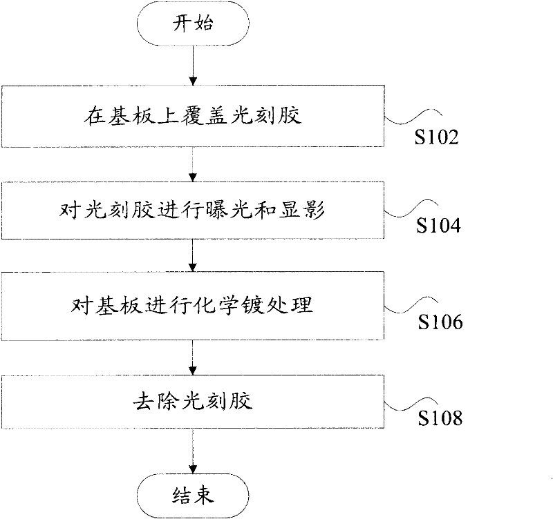
[0032] figure 1 is a flow chart of the manufacturing method of the microfluidic chip according to the first embodiment of the present invention.

[0033] Such as figure 1 As shown, the method includes the following steps S102 to S108:

[0034] Step S102, covering the substrate with photoresist.

[0035] Step S104, exposing and developing the photoresist; the photoresist may be exposed and developed using a predetermined mask.

[0036] Step S106, after exposure and development, the substrate is subjected to electroless plating; wherein, when the substrate is a metal subs...


PUM

PropertyMeasurementUnit
thicknessaaaaaaaaaa
sizeaaaaaaaaaa

Abstract

The invention discloses a substrate mould for a microfluidic chip and a manufacturing method thereof. The method comprises the following steps of: covering photoresist on a substrate; performing exposure and development on the photoresist; performing chemical plating on the substrate; and removing the photoresist. Patterns on the substrate mould can be prevented from being damaged in the process of manufacturing the substrate mould by the method.

Description

technical field [0001] The invention relates to a substrate mold of a microfluidic chip and a manufacturing method thereof. Background technique [0002] The microfluidic chip integrates the basic operation units involved in the fields of chemistry or biology such as sample preparation, reaction, separation, inspection, cell culture, sorting, and lysis into a small chip, forming a network of microchannels. The controllable fluid runs through the whole system to realize various functions of conventional chemical or biological laboratories. [0003] The processing technology of microfluidic analysis chips originated from the microfabrication of semiconductor and integrated circuit chips, but the processing size of the chip channel is much larger than that of large-scale integrated circuits. The size of the chip is about a few square centimeters, and the width and depth of the microchannel are on the order of microns. On the other hand, the selection of chip materials, the des...

Claims


Application Information

Patent Timeline
Patent Type & Authority Applications(China)
IPC IPC(8): G01N35/00G03F7/00
Inventor 许斌刘伟潘龙法姚勤毅
Owner 北京同方光盘股份有限公司
Why Eureka
Try Eureka